 ChipApex | Global Electronic Components Supplier
SEARCH
Search Product
Search Post
— IC芯片 | 连接器 | 传感器 | 被动器件 —
Search productSearch post
— IC芯片 | 连接器 | 传感器 | 被动器件 —
Consult the customer manager about the wholesale price.
consultation hotline:86-132-6715-2157
email:[email protected]
Contact the product manager for consultation. One-stop consultation is available.
Do you want a lower wholesale price? Please send us your inquiry and we will reply immediately.
The IBM 04368CBLBB-30 is a standard SRAM memory integrated circuit with an 8Mbit density. It features a 256K x 36 organization and utilizes 0.25µ CMOS technology. The device operates with a single differential PECL clock and supports synchronous register-latch mode with self-timed late write functionality. Power requirements include a +3.3V supply, ground, and 2.5V VDDQ, while input and output levels are set at 2.5V LVTTL.
Verify the specific speed grade suffix against official IBM documentation to ensure timing compatibility. Confirm that the package type matches the target board layout requirements. Check for RoHS compliance status as indicated in related component records. Ensure power supply voltages align with the specified 3.3V and 2.5V requirements before integration.
Select this component for applications requiring high-density synchronous SRAM with PECL clocking. Consider the 256K x 36 organization for wide data path needs. Evaluate the 0.25µ CMOS process for power efficiency. Verify interface voltage levels match the system's 2.5V LVTTL standards. Assess thermal performance based on the BGA package configuration.
This part belongs to IBM's family of high-performance SRAMs designed for enterprise computing environments. It shares architectural similarities with other models in the series, such as the 0436A8ANLAB, differing primarily in speed grades and organizational configurations. These components support advanced processing tasks in mainframe and distributed systems.
Check for compatible parts within the same IBM SRAM family, such as variants with different speed ratings or organizations. Ensure substitute components maintain the same BGA119 package and electrical specifications. Verify that any alternative maintains the synchronous register-latch mode and PECL clock interface requirements.
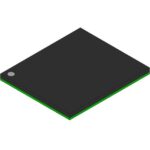 04368CBLBB-30
The activity of extra discounts on wholesale prices is in full swing…
Please fill in your contact information and we will send you the latest wholesale price list.





