 ChipApex | Global Electronic Components Supplier

SEARCH
Search Product
Search Post
— IC芯片 | 连接器 | 传感器 | 被动器件 —
Search productSearch post
— IC芯片 | 连接器 | 传感器 | 被动器件 —
Consult the customer manager about the wholesale price.
consultation hotline:86-132-6715-2157
email:[email protected]
Contact the product manager for consultation. One-stop consultation is available.
Do you want a lower wholesale price? Please send us your inquiry and we will reply immediately.
10M40DCF256C8G is listed in the Field Programmable Gate Array range at ChipApex. The manufacturer field lists Altera. Its product description is IC FPGA 178 I/O 256FBGA. Review the specifications below when checking this part for your BOM.
The Altera 10M40DCF256C8G is a MAX® 10 series Field Programmable Gate Array (FPGA) featuring 40,000 logic elements and 2,500 LAB/CLB units. It integrates 1,290,240 bits of embedded RAM within a 256-LBGA package. The device operates on a core supply voltage range of 1.15V to 1.25V and supports 178 I/O pins. Designed for commercial applications, it functions within a temperature range of 0°C to +85°C TJ. This non-volatile FPGA combines programmable logic with on-chip flash memory, eliminating the need for external configuration devices.
Verify the specific ordering code suffix against the manufacturer's current datasheet to confirm package type and speed grade. Confirm RoHS compliance status and lead times directly with authorized distributors or Intel sales representatives prior to procurement.
Select this model when design requirements include approximately 40k logic resources and significant embedded memory. Ensure the 256-ball LBGA footprint fits the PCB layout constraints. Verify that the commercial temperature range (0°C to +85°C) meets the operational environment specifications.
This component belongs to the Intel MAX® 10 family, which bridges the gap between complex FPGAs and simple CPLDs. It is designed for cost-sensitive, low-power applications where non-vatility and analog integration are critical. It serves as a successor to older MAX/V series devices in mid-range logic applications.
Direct pin-compatible replacements within the same package and speed grade should be verified via official cross-reference tools. Upgrading to higher-density MAX 10 variants may require schematic adjustments due to resource differences.
Explore related parts through Embedded, Integrated Circuits (ICs), all product categories, ChipApex homepage.
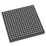 10M40DCF256C8G

The activity of extra discounts on wholesale prices is in full swing…
Please fill in your contact information and we will send you the latest wholesale price list.






