 ChipApex | Global Electronic Components Supplier

SEARCH
Search Product
Search Post
— IC芯片 | 连接器 | 传感器 | 被动器件 —
Search productSearch post
— IC芯片 | 连接器 | 传感器 | 被动器件 —
Consult the customer manager about the wholesale price.
consultation hotline:86-132-6715-2157
email:[email protected]
Contact the product manager for consultation. One-stop consultation is available.
Do you want a lower wholesale price? Please send us your inquiry and we will reply immediately.
10M40DCF484C8G is listed in the Field Programmable Gate Array range at ChipApex. The manufacturer field lists Altera. Its product description is IC FPGA 360 I/O 484FBGA. Review the specifications below when checking this part for your BOM.
The Altera 10M40DCF484C8G is a MAX 10 series Field Programmable Gate Array (FPGA) featuring 40,000 logic elements and integrated non-volatile flash memory. It operates within a supply voltage range of 1.15V to 1.25V and supports up to 360 I/O pins in a 484-ball FBGA package measuring 23x23 mm. The device includes 1,290,240 bits of total RAM and functions at junction temperatures between 0°C and 85°C.
Verify the specific suffix 'DCF' against official Intel/Altera documentation to confirm pinout and feature set accuracy. Check current RoHS compliance status and Moisture Sensitivity Level (MSL 3) requirements before integration. Confirm availability through authorized distributors as standard lead times may vary.
Select this model when non-vatile configuration and moderate logic density are required without external memory components. Compare resource usage against the 10M40DAF variant if flash integration is not needed. Ensure the 484-FBGA package fits the board layout constraints and thermal design specifications.
This component belongs to the Intel MAX 10 family, which utilizes a 55nm process technology. It is designed to replace legacy CPLDs and smaller FPGAs by combining programmable logic with on-chip flash, simplifying system architecture and reducing bill-of-materials count for cost-sensitive applications.
Publicly confirmed substitute part numbers are not available in the provided source material.
Explore related parts through Embedded, Integrated Circuits (ICs), all product categories, ChipApex homepage.

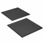 10M40DCF484C8G

The activity of extra discounts on wholesale prices is in full swing…
Please fill in your contact information and we will send you the latest wholesale price list.




