 ChipApex | Global Electronic Components Supplier
SEARCH
Search Product
Search Post
— IC芯片 | 连接器 | 传感器 | 被动器件 —
Search productSearch post
— IC芯片 | 连接器 | 传感器 | 被动器件 —
Consult the customer manager about the wholesale price.
consultation hotline:86-132-6715-2157
email:[email protected]
Contact the product manager for consultation. One-stop consultation is available.
Do you want a lower wholesale price? Please send us your inquiry and we will reply immediately.
The SN74LVC1G08MDBVREP is a single 2-input positive-AND gate from the LVC family, housed in a SOT-23 (DBV) package. It operates within a supply voltage range of 1.65 V to 5.5 V and supports an extended temperature range of -55 °C to 125 °C. The device features a maximum propagation delay of 3.6 ns at 3.3 V, with output drive capabilities of ±32 mA at 4.5 V. It includes Ioff support for partial-power-down mode and meets enhanced manufacturing standards.
Verify the complete part number including suffixes against official Texas Instruments documentation to ensure correct package type and temperature grade. Confirm RoHS compliance status and lead finish specifications prior to procurement. Cross-reference ordering information with current datasheets to validate availability and production status.
Select this component for applications requiring a single AND gate in a compact SOT-23 footprint. Ensure the operating voltage aligns with the 1.65 V to 5.5 V range. Consider the extended temperature rating if deployment environments exceed standard commercial limits. Verify input voltage levels do not exceed absolute maximum ratings during operation.
This device belongs to the SN74LVC1G08-EP series, representing an enhanced product variant of the standard LVC logic family. It is manufactured under controlled baseline conditions with qualification pedigree ensuring reliability. The MDBVREP designation indicates the specific SOT-23 package and reel packaging configuration.
SN74LVC1G08MDCKREP
Yes, the device includes Ioff circuitry that disables outputs to prevent damaging current backflow when powered down.
The maximum propagation delay is 3.6 ns when operating at a supply voltage of 3.3 V.
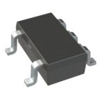 1P1G08MDBVREP
The activity of extra discounts on wholesale prices is in full swing…
Please fill in your contact information and we will send you the latest wholesale price list.





