 ChipApex | Global Electronic Components Supplier

SEARCH
Search Product
Search Post
— IC芯片 | 连接器 | 传感器 | 被动器件 —
Search productSearch post
— IC芯片 | 连接器 | 传感器 | 被动器件 —
Consult the customer manager about the wholesale price.
consultation hotline:86-132-6715-2157
email:[email protected]
Contact the product manager for consultation. One-stop consultation is available.
Do you want a lower wholesale price? Please send us your inquiry and we will reply immediately.
The Altera 1SX280HN1F43E2VGS3 is a Stratix 10 SX Field Programmable Gate Array (FPGA) System on Chip (SoC). It integrates an ARM Cortex-A53 Hard Processor System with high-density FPGA fabric. The device features 2,800,000 logic elements and 933,120 Adaptive Logic Modules (ALMs). It includes 229 Mbit of embedded memory and supports 1,160 I/O pins. The package is a 2912-ball FBGA. Key electrical parameters include a core voltage of 940 mV and an operating temperature range of 0°C to +100°C.
Verify the specific suffix E2 against official Intel/Altera documentation to confirm it denotes the industrial or extended temperature grade variant, as standard datasheets may list generic family specifications. Ensure the ordering information matches the exact pinout and speed grade required for the design. Confirm moisture sensitivity level handling procedures prior to assembly.
Select this component when both high-capacity FPGA logic and an embedded ARM processor are required in a single die. Compare the 2912-ball FBGA package size against board space constraints. Evaluate the 229 Mbit memory capacity against application buffer requirements. Consider the thermal dissipation characteristics of the FBGA-2912 package for the target enclosure.
This part belongs to the Stratix 10 SX family, designed for cost-sensitive applications compared to the GX series. It shares the same HPS architecture but differs in transceiver count and I/O availability. The HN1 designation typically refers to a specific speed grade within the 2800K logic density tier.
Direct replacements within the same package and pinout include other Stratix 10 SX devices with matching logic density, such as the 1SX280HN2F43E2VGS3. Verify that the transceiver count and I/O mapping remain compatible with the existing PCB layout before substituting.
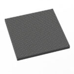 1SX280HN1F43E2VGS3

The activity of extra discounts on wholesale prices is in full swing…
Please fill in your contact information and we will send you the latest wholesale price list.




