 ChipApex | Global Electronic Components Supplier

SEARCH
Search Product
Search Post
— IC芯片 | 连接器 | 传感器 | 被动器件 —
Search productSearch post
— IC芯片 | 连接器 | 传感器 | 被动器件 —
Consult the customer manager about the wholesale price.
consultation hotline:86-132-6715-2157
email:[email protected]
Contact the product manager for consultation. One-stop consultation is available.
Do you want a lower wholesale price? Please send us your inquiry and we will reply immediately.
The Altera 1SX280LN3F43I2LP is a Stratix II Field Programmable Gate Array featuring 279,600 logic elements and 15.6 Mbits of embedded memory. It supports high-speed serial transceivers with data rates up to 3.125 Gbps. The device operates at a core voltage of 1.2V and includes dedicated DSP blocks for complex arithmetic operations. It utilizes a fine-grain architecture optimized for high-performance digital signal processing and networking applications.
Verify the specific suffix codes against official Intel (formerly Altera) documentation to ensure correct temperature range and package variant. Confirm that the component matches the required pinout and electrical specifications for your design. Cross-reference the date code and lot number if traceability is required. Ensure compliance with RoHS directives applicable to the manufacturing batch.
Choose this component when high logic density and integrated transceivers are required for networking or DSP tasks. Evaluate the power consumption profile against thermal constraints in the target enclosure. Consider the availability of development tools and IP cores compatible with the Stratix II family. Assess the need for specific I/O standards supported by the device pins.
This part belongs to the Stratix II family, representing a generation of FPGAs designed for mid-to-high performance applications. It bridges the gap between lower-density devices and the larger Stratix III series. The family introduced enhanced transceiver technology and improved DSP capabilities compared to previous generations.
Direct replacements within the same family include other 1SX280 variants with different package or speed grades. Upgrades may involve Stratix III or IV devices for increased capacity. Verify pin compatibility and software toolchain support before substituting.
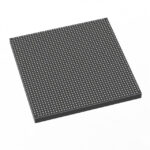 1SX280LN3F43I2LP

The activity of extra discounts on wholesale prices is in full swing…
Please fill in your contact information and we will send you the latest wholesale price list.




