 ChipApex | Global Electronic Components Supplier
SEARCH
Search Product
Search Post
— IC芯片 | 连接器 | 传感器 | 被动器件 —
Search productSearch post
— IC芯片 | 连接器 | 传感器 | 被动器件 —
Consult the customer manager about the wholesale price.
consultation hotline:86-132-6715-2157
email:[email protected]
Contact the product manager for consultation. One-stop consultation is available.
Do you want a lower wholesale price? Please send us your inquiry and we will reply immediately.
The Renesas 2304NZLPGGI8 is a high-performance, low-skew, low-jitter LVCMOS clock buffer with a 1:4 output ratio. It operates within a supply voltage range of 1.8V to 3.3V and supports an industrial temperature range from -40°C to +85°C. The device features low input-to-output propagation delay of 1.8ns at 3.3V and maximum output skew of 40ps. It includes a glitch-free Output Enable function and is packaged in an 8-pin TSSOP (3.1 x 4.4 x 1.0 mm) with 0.65mm pitch.
Verify the specific package variant, as the 2304NZL series is available in SOIC, TSSOP, and DFN packages. Confirm that the PGGI suffix corresponds to the TSSOP-8 tube packaging. Check for RoHS3 compliance and MSL Level 1 status during procurement validation.
Select this component for designs requiring low jitter and skew in LVCMOS clock distribution. Ensure the operating voltage aligns with the 1.8V to 3.3V range. Consider the 1:4 fan-out capability and the availability of the glitch-free enable feature for system synchronization requirements.
The 2304NZLPGGI8 belongs to the Renesas 2304NZL family of LVCMOS clock buffers. This family is designed for high-speed clock distribution in networking and PCI/PCI-X systems, offering low propagation delay and minimal output skew across various package options including TSSOP and SOIC.
The 5PB1110PGGK is listed as a parameter equivalent alternative by distributors, though it differs in technology (LVCMOS vs LVCMOS) and pin count (20-TSSOP vs 8-TSSOP). Verify electrical compatibility and footprint differences before substitution.
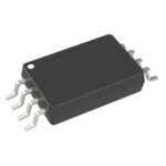 2304NZLPGGI8
The activity of extra discounts on wholesale prices is in full swing…
Please fill in your contact information and we will send you the latest wholesale price list.





