 ChipApex | Global Electronic Components Supplier
SEARCH
Search Product
Search Post
— IC芯片 | 连接器 | 传感器 | 被动器件 —
Search productSearch post
— IC芯片 | 连接器 | 传感器 | 被动器件 —
Consult the customer manager about the wholesale price.
consultation hotline:86-132-6715-2157
email:[email protected]
Contact the product manager for consultation. One-stop consultation is available.
Do you want a lower wholesale price? Please send us your inquiry and we will reply immediately.
The Renesas 2305-1HDCG8 is a zero-delay clock buffer featuring a Phase-Locked Loop (PLL) for low phase noise and high-speed performance. It provides five LVCMOS outputs with a maximum frequency of 133 MHz and zero input-to-output propagation delay. The device operates on a single 3V to 3.6V supply within an industrial temperature range of -40°C to +85°C. Packaged in an 8-pin SOIC, it supports tri-state modes and includes features such as device-to-device skew control and full CMOS output drive capabilities.
Verify the specific suffix 'GI8' against official Renesas documentation to confirm the package type and temperature grade. Confirm RoHS compliance status directly from the manufacturer's current datasheet revision, as regulatory status can change. Ensure the ordering information matches the exact part number to avoid discrepancies in lead times or packaging quantities.
Select this component when zero input-to-output delay is critical for system timing. The 2305-1HDCG8 is suitable for applications requiring five buffered outputs from a single source. Compare the 133 MHz maximum frequency against system requirements. Verify that the 3.3V logic levels are compatible with downstream components.
This part belongs to the IDT 2305 family of zero-delay buffers. The '1H' designation indicates a high-drive version with faster rise and fall times compared to the base model. The 'GI8' suffix specifies the 8-pin SOIC package and the industrial temperature rating. This series is designed for low jitter clock distribution.
The IDT2305-1DCG8 is a related variant within the same family but typically differs in temperature range or drive strength specifications. Cross-reference the exact electrical parameters and package dimensions before substitution. No direct public substitute part numbers are confirmed for this specific suffix combination.
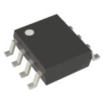 2305-1HDCG8
The activity of extra discounts on wholesale prices is in full swing…
Please fill in your contact information and we will send you the latest wholesale price list.







