 ChipApex | Global Electronic Components Supplier
SEARCH
Search Product
Search Post
— IC芯片 | 连接器 | 传感器 | 被动器件 —
Search productSearch post
— IC芯片 | 连接器 | 传感器 | 被动器件 —
Consult the customer manager about the wholesale price.
consultation hotline:86-132-6715-2157
email:[email protected]
Contact the product manager for consultation. One-stop consultation is available.
Do you want a lower wholesale price? Please send us your inquiry and we will reply immediately.
The Renesas Electronics Corporation 2308B-1HDCG8 is a 3.3V zero-delay clock multiplier IC designed for high-speed clock distribution and multiplication applications. It utilizes a phase-lock loop (PLL) to align the phase between incoming and output clocks, operating within an input frequency range of 10 MHz to 133.3 MHz. The device features eight LVCMOS outputs organized into two banks of four, with separate enable controls for each bank. Key electrical parameters include a maximum output skew of 200 ps and cycle-to-cycle jitter under 200 ps peak-to-peak. It operates at a supply voltage of 3.3V and is housed in a 16-pin SOIC package.
Verify component authenticity through authorized channels as counterfeits exist. Confirm package integrity and lead condition upon receipt. Check datasheet revisions for any pinout or electrical parameter updates before finalizing procurement specifications.
Select this model when a 3.3V supply is required with zero-delay buffering capabilities. Ensure the application frequency falls within the 10 MHz to 133.3 MHz range. Consider the 16-pin SOIC package constraints for PCB layout and thermal management requirements.
This component belongs to the IDT 2308 series of clock multipliers, originally developed by Integrated Device Technology and later acquired by Renesas. It serves as a specialized timing solution for systems needing low-jitter clock multiplication without external RC networks.
Direct substitutes include other variants from the 2308 family such as the 2308B-2HDCG8 or 2308B-5HDCG8, which offer different multiplication ratios. Verify pin compatibility and electrical specifications against the specific design requirements before substitution.
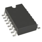 2308B-1HDCG8
The activity of extra discounts on wholesale prices is in full swing…
Please fill in your contact information and we will send you the latest wholesale price list.






