 ChipApex | Global Electronic Components Supplier
SEARCH
Search Product
Search Post
— IC芯片 | 连接器 | 传感器 | 被动器件 —
Search productSearch post
— IC芯片 | 连接器 | 传感器 | 被动器件 —
Consult the customer manager about the wholesale price.
consultation hotline:86-132-6715-2157
email:[email protected]
Contact the product manager for consultation. One-stop consultation is available.
Do you want a lower wholesale price? Please send us your inquiry and we will reply immediately.
The Renesas 2309-1HDCGI is a low phase noise, high-speed PLL-based zero delay buffer designed for clock distribution. It accepts one LVTTL input and provides nine LVTTL outputs with a 1:9 ratio. The device operates at frequencies up to 133 MHz within a 3V to 3.6V supply range. Key electrical parameters include a maximum propagation delay of 0 ps, output skew under 250 ps, and cycle-to-cycle jitter below 200 ps. It is housed in a 16-SOIC package and supports commercial temperature operation from 0°C to +70°C.
Verify the suffix 'I' indicates industrial temperature range (-40°C to 85°C) or confirm if it denotes a specific variant, as standard datasheets often list 'G' for commercial (0°C to 70°C). Ensure RoHS compliance status matches current manufacturing notices. Check moisture sensitivity level (MSL 3) requirements for storage and handling before assembly.
Select this component when a single clock source must drive multiple loads with minimal skew. Compare against the 2309A series for drive strength differences; the -1H variant offers higher drive capability. Confirm that the LVTTL input/output voltage levels match the system logic requirements. Verify package availability in SOIC-16 versus TSSOP options based on board space constraints.
This part belongs to the IDT/Renesas 2309 family of zero delay buffers. It is functionally similar to the 2305A but expanded to 16 pins to support nine outputs. The device is widely used in telecommunications and computing infrastructure for clock fan-out applications.
The PL123-09SC-R by Microchip Technology is listed as a similar alternative. Verify pinout compatibility and electrical specifications before substitution.
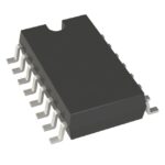 2309-1HDCGI
The activity of extra discounts on wholesale prices is in full swing…
Please fill in your contact information and we will send you the latest wholesale price list.





