 ChipApex | Global Electronic Components Supplier
SEARCH
Search Product
Search Post
— IC芯片 | 连接器 | 传感器 | 被动器件 —
Search productSearch post
— IC芯片 | 连接器 | 传感器 | 被动器件 —
Consult the customer manager about the wholesale price.
consultation hotline:86-132-6715-2157
email:[email protected]
Contact the product manager for consultation. One-stop consultation is available.
Do you want a lower wholesale price? Please send us your inquiry and we will reply immediately.
The Renesas 2309A-1HDCG8 is a high-speed, low-phase-noise PLL-based zero delay clock buffer designed for distributing reference clocks. It accepts one LVCMOS input and provides nine LVCMOS outputs with a 1:9 ratio. Operating at 3.3V, the device supports frequencies from 10MHz to 133MHz. Key electrical parameters include an output skew of less than 250ps and cycle-to-cycle jitter under 200ps. The component is housed in a 16-pin SOIC package (code DCG) and operates within a commercial temperature range of 0°C to +70°C.
Verify the specific suffix '8' indicates tape-and-reel packaging when sourcing. Confirm the 'A' variant designation against current datasheets to ensure compatibility with required drive strength and frequency specifications. Check moisture sensitivity level (MSL 3) requirements for storage and handling procedures prior to assembly.
Select this part for applications requiring a single input to fan out to nine outputs without external components. Ensure the system voltage matches the 3.3V supply requirement. Compare against the standard 2309A-1 if lower drive strength is sufficient, or consider the -1H version for faster rise/fall times if specified by the design constraints.
This component belongs to the 2309A series of zero delay buffers manufactured by Renesas Electronics. It serves as a clock distribution solution derived from legacy ICS technology acquired by Renesas. The device is functionally similar to other members of the family but is distinguished by its specific pinout, package type, and output count configuration.
The IDT2309A-1HDCG8 is a direct equivalent part number. Verify pin compatibility and electrical characteristics against the current Renesas datasheet before substituting.
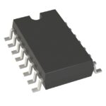 2309A-1HDCG8
The activity of extra discounts on wholesale prices is in full swing…
Please fill in your contact information and we will send you the latest wholesale price list.






