 ChipApex | Global Electronic Components Supplier
SEARCH
Search Product
Search Post
— IC芯片 | 连接器 | 传感器 | 被动器件 —
Search productSearch post
— IC芯片 | 连接器 | 传感器 | 被动器件 —
Consult the customer manager about the wholesale price.
consultation hotline:86-132-6715-2157
email:[email protected]
Contact the product manager for consultation. One-stop consultation is available.
Do you want a lower wholesale price? Please send us your inquiry and we will reply immediately.
The Renesas 23S05E-1DCGI8 is a 3.3V zero-delay clock buffer designed for high-speed digital systems. It utilizes a Phase-Locked Loop (PLL) to generate outputs with minimal input-to-output delay, ensuring precise timing alignment. The device supports frequencies from 10 MHz to 133 MHz and provides five LVCMOS outputs. Key electrical parameters include a maximum propagation delay of 0 ps, an output skew of less than 250 ps, and a core operating voltage of 3.3 V. It operates within an industrial temperature range of -40°C to +85°C and is housed in an 8-pin SOIC package.
Verify the specific suffix 'E' against official Renesas documentation, as standard listings often reference the 23S05-1HDCGI8 or 23S05-1DCGI8 variants. Confirm that the 'E' designation does not imply a restricted automotive qualification or a distinct pinout if it differs from the commercial grade. Ensure the SOIC-8 package dimensions match the required PCB footprint before ordering.
Select this component when zero input-to-output delay is critical for system timing integrity. It is suitable for applications requiring fan-out of a single reference clock to multiple synchronous devices. Compare the 250 ps inter-output skew against system tolerance limits. Consider the 3.3V supply requirement and ensure compatibility with downstream LVCMOS logic levels.
This part belongs to the IDT/Renesas 23S05 family of zero-delay buffers. These devices are engineered to replace crystal oscillators by buffering a lower-frequency reference clock while maintaining phase coherence. The 23S05 series is widely used in networking and computing infrastructure where jitter reduction and skew minimization are paramount for data integrity.
The 23S05-1HDCGI8 is a documented equivalent within the same family, offering similar zero-delay functionality. Verify if the 'H' variant's higher drive strength is necessary for the specific load conditions. Cross-reference pinouts to ensure direct replacement compatibility without schematic modifications.
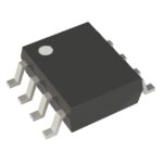 23S05E-1DCGI8
The activity of extra discounts on wholesale prices is in full swing…
Please fill in your contact information and we will send you the latest wholesale price list.





