 ChipApex | Global Electronic Components Supplier
SEARCH
Search Product
Search Post
— IC芯片 | 连接器 | 传感器 | 被动器件 —
Search productSearch post
— IC芯片 | 连接器 | 传感器 | 被动器件 —
Consult the customer manager about the wholesale price.
consultation hotline:86-132-6715-2157
email:[email protected]
Contact the product manager for consultation. One-stop consultation is available.
Do you want a lower wholesale price? Please send us your inquiry and we will reply immediately.
The Renesas 23S08-4DCGI is a 3.3V zero-delay clock multiplier belonging to the 23S08 family, designed for high-speed clock distribution and multiplication applications. It operates within an input frequency range of 10 MHz to 133 MHz using LVCMOS inputs. The device features eight LVCMOS outputs organized into two banks, providing a multiply/divide value of 1. Key electrical specifications include a maximum cycle-to-cycle jitter of 200 ps and output skew of 200 ps. It supports spread spectrum input compatibility and is housed in a 16-pin TSSOP package with dimensions of 5.0 x 4.4 x 1.0 mm.
Verify component status as the 23S08 series may be obsolete or end-of-life. Confirm package type (TSSOP) and lead-free status (Pb Free Yes). Check moisture sensitivity level (MSL 1) requirements for storage and handling. Ensure availability through authorized distributors as stock levels vary.
Select this part for single-input, eight-output LVCMOS clock distribution needs. Verify that the 1x multiplication factor meets system timing requirements. Consider the TSSOP-16 package constraints for PCB layout. Compare against other 23S08 variants if different multiplication ratios or drive strengths are required.
The 23S08-4DCGI is part of the IDT/Renesas 23S08 family of zero-delay buffers. It shares core architecture with variants like 23S08-1HPGG and 23S08-2HDCG but differs in package and specific configuration suffixes. It is distinct from the 2308 series which offers different multiplication options.
Direct substitutes within the same family include 23S08-1HPGG (TSSOP) and 23S08-2HDCG (SOIC), though pinout and package dimensions differ. Verify functional equivalence regarding jitter and skew specifications before substitution.
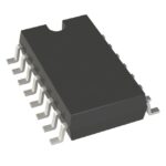 23S08-4DCGI
The activity of extra discounts on wholesale prices is in full swing…
Please fill in your contact information and we will send you the latest wholesale price list.





