 ChipApex | Global Electronic Components Supplier
SEARCH
Search Product
Search Post
— IC芯片 | 连接器 | 传感器 | 被动器件 —
Search productSearch post
— IC芯片 | 连接器 | 传感器 | 被动器件 —
Consult the customer manager about the wholesale price.
consultation hotline:86-132-6715-2157
email:[email protected]
Contact the product manager for consultation. One-stop consultation is available.
Do you want a lower wholesale price? Please send us your inquiry and we will reply immediately.
The Renesas 23S08E-2DCGI8 is a discontinued 3.3V zero-delay clock multiplier compatible with spread spectrum inputs. It features one LVCMOS input and eight LVCMOS outputs, supporting frequencies from 10 MHz to 133 MHz. The device provides multiply/divide values of 1 or 2, with a maximum core-to-core jitter of 200 ps peak-to-peak and output skew of 200 ps. Packaged in a 16-pin SOIC (DCG) tube, it operates within a commercial temperature range of 0°C to 70°C.
This component is officially listed as obsolete by the manufacturer. Availability is restricted to remaining stock held by distributors such as Avnet and Flip Electronics. Verification of lot dates and storage conditions is critical due to the end-of-life status. Standard procurement channels may not guarantee new production units.
Designers should verify that the 10–133 MHz frequency range meets system requirements. The LVCMOS I/O levels must align with downstream logic voltage tolerances. Consider the 200 ps jitter specification against the sensitivity of connected receivers. Alternative solutions from the Femtoclock family may offer updated availability and enhanced performance metrics.
The 23S08 series belongs to Renesas' legacy clock multiplier portfolio, designed for zero-delay buffering applications. This specific variant utilizes a 16-pin SOIC package. It serves as a foundational component for distributing reference clocks across multiple subsystems in embedded electronics.
Publicly confirmed substitute part numbers are not available in the provided documentation. Engineers should consult current Renesas Femtoclock product lines for functional equivalents with active manufacturing support.
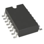 23S08E-2DCGI8
The activity of extra discounts on wholesale prices is in full swing…
Please fill in your contact information and we will send you the latest wholesale price list.





