 ChipApex | Global Electronic Components Supplier
SEARCH
Search Product
Search Post
— IC芯片 | 连接器 | 传感器 | 被动器件 —
Search productSearch post
— IC芯片 | 连接器 | 传感器 | 被动器件 —
Consult the customer manager about the wholesale price.
consultation hotline:86-132-6715-2157
email:[email protected]
Contact the product manager for consultation. One-stop consultation is available.
Do you want a lower wholesale price? Please send us your inquiry and we will reply immediately.
The Renesas 23S09T-1DCG8 is a high-speed phase-locked loop (PLL) clock buffer designed for zero-delay clock distribution. It accepts one reference input and drives nine outputs, organized into two banks of four and one bank of five. The device operates within a frequency range of 10MHz to 133MHz at a 3.3V supply voltage. Key electrical parameters include an output skew of less than 250ps and cycle-to-cycle jitter below 200ps. The -1H suffix indicates a high-drive version with faster rise and fall times compared to the standard -1 variant. It features separate output enables for each bank and enters a low-power tri-state mode when no input clock is present.
Verify the specific suffix 'T' against official Renesas documentation, as it may indicate tape-and-reel packaging or a specific moisture sensitivity level. Confirm RoHS compliance status, as older variants of this family have been noted as non-compliant in some distributor records. Check for active manufacturing status, as certain versions of the 23S09 family have reached end-of-life.
Select the -1H variant over the standard -1 if higher drive strength and faster edge rates are required for signal integrity at 133MHz. Ensure the design supports the 3.3V VDD operating range. Verify that the PCB layout accommodates the SOIC-16 package dimensions (9.9 x 3.9 x 1.5 mm) and pitch requirements.
The 23S09 series is part of Renesas' zero-delay buffer lineup, serving as a 16-pin expansion of the 23S05. It utilizes on-chip PLL feedback from the CLKOUT pad to lock to the REF pin input. This family is characterized for both commercial (0°C to 70°C) and industrial (-40°C to 85°C) temperature ranges, providing flexibility for various environmental conditions.
The IDT23S09-1HPG8 is a documented equivalent offering similar zero-delay buffering in a TSSOP package. Note that the IDT variant has been marked as obsolete in some sources; verify current availability and RoHS status before substitution.
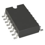 23S09T-1DCG8
The activity of extra discounts on wholesale prices is in full swing…
Please fill in your contact information and we will send you the latest wholesale price list.





