 ChipApex | Global Electronic Components Supplier
SEARCH
Search Product
Search Post
— IC芯片 | 连接器 | 传感器 | 被动器件 —
Search productSearch post
— IC芯片 | 连接器 | 传感器 | 被动器件 —
Consult the customer manager about the wholesale price.
consultation hotline:86-132-6715-2157
email:[email protected]
Contact the product manager for consultation. One-stop consultation is available.
Do you want a lower wholesale price? Please send us your inquiry and we will reply immediately.
The Renesas 2510CGLFT is a high-performance, low-skew, low-jitter clock driver utilizing phase-lock loop (PLL) technology. It aligns the CLKIN signal with the CLKOUT signal in both phase and frequency, specifically designed for synchronous SDRAM applications. The device operates at 3.3V VCC and distributes one clock input to ten outputs, supporting frequencies from 25MHz to 175MHz. It meets or exceeds PC133 registered DIMM specifications. The component is housed in a plastic 24-pin TSSOP package with dimensions of 7.8 x 4.4 x 1.0 mm and a lead pitch of 0.65 mm.
Verify the specific suffix 'GLFT' indicates lead-free composition and tape-and-reel packaging. Confirm current availability status as distribution channels may list obsolete variants like the non-lead-free 2510CG. Ensure the order specifies the reel quantity of 3000 units if bulk packaging is required for surface mount assembly.
Select this component when a 1:10 fanout buffer with integrated PLL jitter attenuation is required for memory subsystems. It is suitable for designs needing spread spectrum clocking capabilities. Verify that the 3.3V supply voltage and 24-TSSOP footprint match the target PCB layout constraints.
The 2510CGLFT belongs to the 2510C family of clock drivers. The 'G' suffix typically denotes lead-free construction, while 'LF' confirms RoHS compliance. The 'T' suffix indicates tube packaging for the base model, but the 'FT' variant specifically denotes tape-and-reel packaging for automated assembly processes.
Direct pin-compatible replacements within the same family include the 2510CGLF (tube packaging). For lead-free requirements, verify the 2510CGLFT against other active inventory. Cross-model substitution requires careful evaluation of electrical parameters and package dimensions.
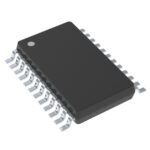 2510CGLFT
The activity of extra discounts on wholesale prices is in full swing…
Please fill in your contact information and we will send you the latest wholesale price list.





