 ChipApex | Global Electronic Components Supplier
SEARCH
Search Product
Search Post
— IC芯片 | 连接器 | 传感器 | 被动器件 —
Search productSearch post
— IC芯片 | 连接器 | 传感器 | 被动器件 —
Consult the customer manager about the wholesale price.
consultation hotline:86-132-6715-2157
email:[email protected]
Contact the product manager for consultation. One-stop consultation is available.
Do you want a lower wholesale price? Please send us your inquiry and we will reply immediately.
The Microchip Technology 25CSM04-I/SN is a 4-Mbit SPI Serial EEPROM organized as 524,288 x 8 bytes. It operates within a voltage range of 2.5V to 5.5V and supports clock frequencies up to 8 MHz at VCC ≥ 3.0V or 5 MHz at VCC ≥ 2.5V. The device features a Security Register with a preprogrammed 128-bit serial number and a 256-byte user-programmable lockable ID page. Built-in ECC logic corrects single-bit errors per four-byte read. It offers configurable write protection via Legacy Block Protection or Enhanced Memory Partitioning modes. The component provides over one million erase/write cycles and data retention exceeding 100 years.
Verify that the ordering suffix 'I' corresponds to the Industrial temperature range (-40°C to +85°C). Confirm the package type matches the SOIC-8 specification. Ensure the specific revision level aligns with your design requirements. Cross-reference the JEDEC standard compliance for identification registers if system integration depends on it. Validate voltage specifications against your power supply rails.
Select this component when high reliability and security are required alongside standard EEPROM functionality. The built-in ECC ensures data integrity during reads, while the flexible write protection schemes allow for robust configuration management. The inclusion of a unique serial number simplifies manufacturing serialization processes. Consider the enhanced partitioning features if distinct memory zones require different protection levels.
The 25CSM04 belongs to Microchip's CS series of SPI Serial EEPROMs, which are optimized for applications requiring secure and dependable nonvolatile storage. This series integrates advanced security features like unique serial numbers and lockable ID pages directly into the memory structure. The devices support broad voltage ranges and offer various package options to suit different form factors.
Check datasheets for other 25CSMxx models in the CS series for capacity variations. Verify compatibility with existing SPI interface protocols and voltage levels. Ensure replacement parts maintain similar ECC and write protection feature sets if these are critical to the application design.
The built-in ECC logic can correct up to one incorrectly read bit within every four bytes read out from the memory array. It also includes a flag in the STATUS register to report detected and corrected errors.
Legacy mode uses Block Protection bits in the STATUS register to protect quarter, half, or entire arrays. Enhanced mode segments memory into independent partitions defined by Memory Partition Registers, allowing unique protection behavior for each zone.
Yes, the user-programmable portion of the Security Register can be permanently write-protected via a software sequence, preventing any further alterations to the data.
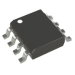 25CSM04-I/SN
The activity of extra discounts on wholesale prices is in full swing…
Please fill in your contact information and we will send you the latest wholesale price list.





