 ChipApex | Global Electronic Components Supplier
SEARCH
Search Product
Search Post
— IC芯片 | 连接器 | 传感器 | 被动器件 —
Search productSearch post
— IC芯片 | 连接器 | 传感器 | 被动器件 —
Consult the customer manager about the wholesale price.
consultation hotline:86-132-6715-2157
email:[email protected]
Contact the product manager for consultation. One-stop consultation is available.
Do you want a lower wholesale price? Please send us your inquiry and we will reply immediately.
The Microchip Technology 25LC080A-I/P is an 8 Kbit (1024 x 8-bit) Serial Electrically Erasable PROM featuring a 16-byte page size. It operates within a supply voltage range of 2.5 V to 5.5 V and supports a maximum clock frequency of 10 MHz via a standard SPI-compatible interface. The device utilizes low-power CMOS technology, offering high reliability with over 1,000,000 erase/write cycles and data retention exceeding 200 years. It is housed in an 8-lead PDIP package and functions reliably across an industrial temperature range of -40 °C to +85 °C.
Verify the specific suffix 'I' confirms the industrial temperature range (-40 °C to +85 °C) and 'P' indicates the 8-lead PDIP package. Confirm RoHS compliance and lead-free status as specified in the datasheet. Ensure the ordering part number matches the exact 'A' version requirements for the 16-byte page size structure.
Select this component when a non-volatile memory solution requires a simple SPI interface and robust write protection features. It is suitable for applications needing moderate speed up to 10 MHz and high endurance. Consider alternative packages like MSOP or TSSOP if surface-mount assembly is required instead of through-hole mounting.
This device belongs to the 25XX080A/B family of 8 Kbit Serial EEPROMs manufactured by Microchip Technology. The 'LC' designation specifically denotes operation at a minimum supply voltage of 2.5 V, distinguishing it from the 'AA' variant which supports lower voltages down to 1.8 V. All variants share identical pinouts and core functionality.
Direct functional substitutes within the same package include the 25LC080B-I/P, which offers a 32-byte page size instead of 16 bytes. Other compatible options are the 25AA080A-I/P for lower voltage applications or the 25LC080D-E/P for extended temperature ranges, provided interface and voltage specifications align.
The HOLD pin allows the user to pause transmission to the device mid-sequence without resetting the serial pointer. When pulled low while SCK is low, inputs are ignored until the pin is raised high again.
The Write Enable Latch must be set via the WREN instruction before any write operation can occur. It resets automatically after power-up, successful write completion, or execution of the WRDI instruction to prevent accidental data corruption.
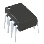 25LC080A-I/P
The activity of extra discounts on wholesale prices is in full swing…
Please fill in your contact information and we will send you the latest wholesale price list.





