 ChipApex | Global Electronic Components Supplier

SEARCH
Search Product
Search Post
— IC芯片 | 连接器 | 传感器 | 被动器件 —
Search productSearch post
— IC芯片 | 连接器 | 传感器 | 被动器件 —
Consult the customer manager about the wholesale price.
consultation hotline:86-132-6715-2157
email:[email protected]
Contact the product manager for consultation. One-stop consultation is available.
Do you want a lower wholesale price? Please send us your inquiry and we will reply immediately.
The Microchip Technology 25LC128-I/P is a 128 Kbit Serial Electrically Erasable PROM featuring an SPI-compatible interface. It utilizes a 16,384 x 8-bit organization with a 64-byte page size. The device operates within a voltage range of 2.5V to 5.5V and supports a maximum clock frequency of 10 MHz at higher voltages. It offers industrial temperature coverage from -40°C to +85°C. Key electrical characteristics include a standby current of 5 µA and self-timed erase/write cycles completing in 5 ms maximum.
Verify the specific suffix 'I' confirms the Industrial temperature range (-40°C to +85°C) and 'P' denotes the PDIP package. Confirm the voltage range requirement aligns with the 2.5V minimum specification for the LC variant, distinct from the AA variant's 1.8V minimum. Ensure compatibility with the host SPI controller's voltage levels and clock speed limitations before integration.
Select this component when an SPI interface is required for 128 Kbit storage with industrial temperature tolerance. The 25LC128 differs from the 25AA128 by its 2.5V minimum supply voltage, making it suitable for 3.3V or 5V systems but potentially incompatible with strict 1.8V-only designs. Consider the PDIP package for through-hole prototyping or manufacturing needs where surface mount options are not preferred.
This part belongs to the 25XX128 family of serial EEPROMs from Microchip Technology. It shares functional similarities with the 25AA128 but differs in supply voltage specifications. The family supports multiple packages including DFN, SOIC, and TSSOP, providing flexibility for various PCB layout requirements while maintaining consistent electrical performance across the series.
The 25AA128-I/P is a functional substitute within the same family, differing primarily in the minimum operating voltage (1.8V vs 2.5V). Verify that the system voltage remains above 2.5V if replacing the 25LC128 with the 25AA128, although the latter offers broader voltage compatibility. Other 128Kbit SPI EEPROMs may require firmware adjustments due to potential differences in instruction sets or timing parameters.
The HOLD pin allows the user to pause serial communication without resetting the sequence. When pulled low while SCK is low, the SI, SCK, and SO pins enter a high-impedance state. Communication resumes when HOLD is brought high while SCK is low.
The Write Enable Latch must be set via the WREN instruction before any write operation can be completed. It resets automatically after power-up, successful execution of WRDI, WRSR, or WRITE instructions, ensuring data integrity against accidental writes.
Yes, the Block Protection bits (BP0 and BP1) in the STATUS register allow protection of none, the upper 1/4, the upper 1/2, or all of the memory array. This protection is nonvolatile and persists until changed by a valid WRSR sequence.
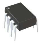 25LC128-I/P

The activity of extra discounts on wholesale prices is in full swing…
Please fill in your contact information and we will send you the latest wholesale price list.





