ChipApex | Global Electronic Components Supplier
SEARCH
Search Product
Search Post
— IC芯片 | 连接器 | 传感器 | 被动器件 —
Search productSearch post
— IC芯片 | 连接器 | 传感器 | 被动器件 —
Consult the customer manager about the wholesale price.
consultation hotline:86-132-6715-2157
email:[email protected]
Contact the product manager for consultation. One-stop consultation is available.
Do you want a lower wholesale price? Please send us your inquiry and we will reply immediately.
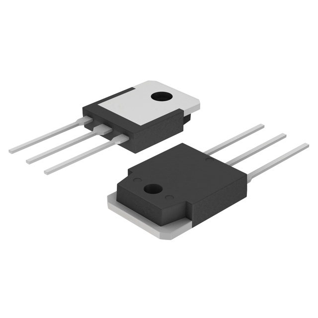
The Toshiba 2SK2967 is a silicon N-channel MOS field-effect transistor utilizing π-MOSV technology, designed for DC-DC converters, relay drives, and motor drives. It features a drain-source voltage rating of 250 V and a continuous drain current of 30 A at 25°C case temperature. The device exhibits a typical drain-source ON resistance of 48 mΩ and a forward transfer admittance of 30 S. Key electrical characteristics include a gate threshold voltage range of 1.5 to 3.5 V and a maximum gate leakage current of ±10 μA. Thermal performance includes a channel-to-case thermal resistance of 0.833 °C/W.
Verify the specific ordering suffix and lot number markings on the component body to confirm environmental compliance status, such as RoHS compatibility. Consult official Toshiba documentation or authorized distributors for current availability and exact package specifications. Ensure that design parameters remain within absolute maximum ratings to maintain reliability. Review the Toshiba Semiconductor Reliability Handbook for derating guidelines and application precautions before integration into final products.
Select this component for applications requiring a 250 V N-channel MOSFET with moderate current handling capabilities up to 30 A. Consider the thermal resistance values when designing heat dissipation strategies, particularly for continuous operation. Evaluate the gate charge requirements against driver capabilities to ensure adequate switching speeds. Verify that the operating voltage and current limits align with the system's peak and steady-state demands to prevent overstress.
This device belongs to Toshiba's lineup of silicon N-channel MOS type field effect transistors. It is packaged in a JEDEC-compatible outline, specifically identified as 2-16C1B, which facilitates mounting on heat sinks via the drain terminal. The component is intended for general electronics applications, including industrial and consumer equipment, provided it is not used in unintended high-reliability sectors without explicit permission.
No public confirmed substitute part numbers are documented in the source material. Users must consult Toshiba sales representatives or official replacement guides for compatible alternatives. Do not assume cross-compatibility with other manufacturers' parts without verifying pinout, electrical ratings, and thermal characteristics against the original specifications.
The maximum drain-source voltage (VDSS) is rated at 250 V.
The gate threshold voltage (Vth) ranges from 1.5 V to 3.5 V under test conditions of VDS = 10 V and ID = 1 mA.
The transistor is an electrostatic-sensitive device; users are advised to handle it with caution to prevent damage from static electricity.
 2SK2967(F)
The activity of extra discounts on wholesale prices is in full swing…
Please fill in your contact information and we will send you the latest wholesale price list.