ChipApex | Global Electronic Components Supplier
SEARCH
Search Product
Search Post
— IC芯片 | 连接器 | 传感器 | 被动器件 —
Search productSearch post
— IC芯片 | 连接器 | 传感器 | 被动器件 —
Consult the customer manager about the wholesale price.
consultation hotline:86-132-6715-2157
email:[email protected]
Contact the product manager for consultation. One-stop consultation is available.
Do you want a lower wholesale price? Please send us your inquiry and we will reply immediately.
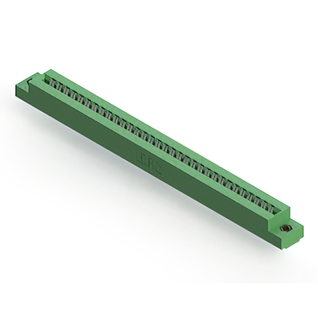
The EDAC Inc. 306-032-421-107 is a standard card edge connector receptacle featuring 64 positions with a 3.96 mm (0.156 inch) pitch. Designed for dual-edge board insertion, it utilizes a copper alloy contact material with tin plating to ensure reliable signal transmission. The component supports a current rating of 5 A and operates within a temperature range of -40°C to +105°C. It employs a solder pin termination style for secure panel mounting and is constructed from thermoplastic polyester insulation.
Verify the specific ordering suffix against the manufacturer's official datasheet to confirm exact plating thickness and flange dimensions. Ensure compatibility with the target PCB thickness specifications before procurement. Confirm RoHS compliance status through the latest certified documentation provided by EDAC Inc. to meet regulatory requirements for your specific manufacturing region.
Select this component when a high-density 64-position interface is required for dual-edge cards. The 3.96 mm pitch accommodates standard board widths while maintaining structural integrity. Consider the tin plating option if lead-free soldering processes are mandated. Verify that the vertical mounting style aligns with the chassis layout constraints and thermal management requirements of the final assembly.
This part belongs to the EDAC 306 series of standard card edge connectors. The series offers various position counts and termination styles to support diverse electronic integration needs. The 306-032-421-107 specifically addresses applications requiring dual-edge connectivity with a moderate pin count, balancing space efficiency with connection reliability in compact enclosures.
Consult the EDAC 306 Series Ordering Guide for direct substitutes with differing position counts or termination types. Cross-reference mechanical drawings to verify flange diameter and mounting hole alignment. Ensure any alternative maintains the same 3.96 mm pitch and current rating to preserve system performance without redesigning the host PCB footprint.
 306-032-421-107
The activity of extra discounts on wholesale prices is in full swing…
Please fill in your contact information and we will send you the latest wholesale price list.