 ChipApex | Global Electronic Components Supplier

SEARCH
Search Product
Search Post
— IC芯片 | 连接器 | 传感器 | 被动器件 —
Search productSearch post
— IC芯片 | 连接器 | 传感器 | 被动器件 —
Consult the customer manager about the wholesale price.
consultation hotline:86-132-6715-2157
email:[email protected]
Contact the product manager for consultation. One-stop consultation is available.
Do you want a lower wholesale price? Please send us your inquiry and we will reply immediately.
The Microchip Technology 34VL02T/ST is a 2 Kbit (256 x 8) Electrically Erasable PROM featuring a 2-Wire I²C compatible serial interface. It operates on a single supply voltage ranging from 1.5V to 3.6V, with a maximum clock frequency of 400 kHz (100 kHz for VCC < 1.8V). The device utilizes low-power CMOS technology, drawing typical read currents of 1 mA and standby currents of 100 nA. It includes a 16-byte page write buffer and supports up to eight cascaded devices via chip select pins.
Verify that the ordering suffix 'T' corresponds to the TSSOP-8 package type as specified in the datasheet. Confirm the temperature grade matches the required operational range of -20°C to +85°C. Ensure compatibility with the 1.5V to 3.6V supply voltage constraints. Check RoHS compliance status if required by manufacturing standards. Validate pin configurations against the specific TSSOP footprint requirements.
Select this component when a 2 Kbit capacity is sufficient for system requirements. Choose this part for designs operating within the 1.5V to 3.6V voltage range. Consider this device if I²C interface compatibility is mandatory. Evaluate the need for dual software write-protection features for the lower memory half. Assess whether the TSSOP-8 surface mount package fits the board layout constraints.
The 34VL02 belongs to the 34VL series of 2 Kbit serial EEPROMs manufactured by Microchip Technology. This series is characterized by its low-voltage operation and robust write-protection schemes. The device integrates high-voltage detection circuits to ensure reliable programming cycles across the specified voltage range.
Consult the manufacturer's documentation for direct cross-reference part numbers. Verify electrical specifications and pinout compatibility before substituting. Ensure any alternative device supports the same I²C protocol and voltage levels.
The PSWP command permanently locks the first 128 bytes (addresses 00h-7Fh) of the array. Once enabled, this protection cannot be reversed through any instruction, power cycling, or the state of the WP pin.
The A0 pin serves a dual purpose: it acts as a chip select address input and detects the high voltage (VHV) required to execute software write-protect commands like SWP and CSWP.
No, sequential reads cannot cross device boundaries. While up to eight devices can be cascaded to expand address space, each device must be addressed individually for continuous reading operations.
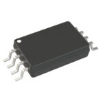 34VL02T/ST

The activity of extra discounts on wholesale prices is in full swing…
Please fill in your contact information and we will send you the latest wholesale price list.





