 ChipApex | Global Electronic Components Supplier
SEARCH
Search Product
Search Post
— IC芯片 | 连接器 | 传感器 | 被动器件 —
Search productSearch post
— IC芯片 | 连接器 | 传感器 | 被动器件 —
Consult the customer manager about the wholesale price.
consultation hotline:86-132-6715-2157
email:[email protected]
Contact the product manager for consultation. One-stop consultation is available.
Do you want a lower wholesale price? Please send us your inquiry and we will reply immediately.
The 49FCT20805PYGI8 is a dual 1:5 clock driver and distribution buffer manufactured by Renesas Electronics. It operates on a single 2.3V to 2.7V supply voltage and supports CMOS and LVTTL input/output logic levels. The device features two independent driver banks, each providing a 1:5 fanout with a maximum operating frequency of 166 MHz. Packaged in a 20-SSOP (5.30mm wide) surface-mount format, it functions within an industrial temperature range of -40°C to +85°C. This component is designed for high-speed clock distribution applications requiring low skew and signal integrity.
The manufacturer lists the 49FCT20805PYGI as End-of-Life (EOL). Verification of the specific '8' suffix variant status is required, as official documentation primarily references the tube-packaged part. Confirm current production availability and lead times directly with Renesas or authorized distributors before design finalization.
Select this component for designs requiring dual 1:5 clock buffering at frequencies up to 166 MHz. Ensure the system power rail strictly adheres to the 2.3V–2.7V specification. Verify that the PCB layout accommodates the 20-SSOP package dimensions. Check if the LVTTL/CMOS compatibility meets the interface requirements of the receiving devices.
This part belongs to the 49FCT series of fast CMOS clock drivers. It is functionally similar to the IDT49FCT20805. The '8' suffix typically indicates tape-and-reel packaging, whereas the base model often refers to tube packaging. Both variants share identical electrical characteristics and pinouts.
The maximum operating frequency is 166 MHz.
No, the device does not support differential inputs or outputs; it uses single-ended CMOS/LVTTL signaling.
The device requires a single supply voltage between 2.3V and 2.7V.
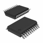 49FCT20805PYGI8
The activity of extra discounts on wholesale prices is in full swing…
Please fill in your contact information and we will send you the latest wholesale price list.





