 ChipApex | Global Electronic Components Supplier
SEARCH
Search Product
Search Post
— IC芯片 | 连接器 | 传感器 | 被动器件 —
Search productSearch post
— IC芯片 | 连接器 | 传感器 | 被动器件 —
Consult the customer manager about the wholesale price.
consultation hotline:86-132-6715-2157
email:[email protected]
Contact the product manager for consultation. One-stop consultation is available.
Do you want a lower wholesale price? Please send us your inquiry and we will reply immediately.
The 49FCT3805AQG8 is a dual clock fanout buffer manufactured by Renesas Electronics. It features two independent buffers, each providing a 1:5 input-to-output ratio for clock distribution. The device operates on a single 3V to 3.6V power supply and supports CMOS and LVTTL input/output logic levels. It is housed in a 20-SSOP package with a width of 0.154 inches (3.90mm). The component is rated for an industrial operating temperature range of -40°C to +85°C.
Verify the specific suffix 'QGI8' against the manufacturer's current datasheet to confirm package dimensions and pinout compatibility. Ensure that the required operating temperature range aligns with the industrial specification (-40°C to +85°C) rather than commercial variants. Confirm RoHS compliance status through official documentation prior to integration into regulated assemblies.
Select this component when a dual-channel clock driver with five outputs per channel is required. It is appropriate for designs utilizing 3.3V logic families. Consider alternative packages if board space constraints differ from the SSOP form factor. Validate signal integrity requirements against the device's drive capability specifications found in the official electrical characteristics tables.
This part belongs to the 49FCT series of high-speed clock drivers. It serves as a non-inverting buffer built using advanced dual metal CMOS technology. The device is designed to replace older FCT series components while offering improved performance metrics. It functions as a critical timing element in complex digital circuits requiring multiple synchronized clock domains.
The 49FCT3805ASOGI8 is a documented substitute part number offering similar functionality in a SOIC package. Verify pinout compatibility and physical footprint differences before swapping between SSOP and SOIC variants.
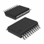 49FCT3805AQG8
The activity of extra discounts on wholesale prices is in full swing…
Please fill in your contact information and we will send you the latest wholesale price list.






