 ChipApex | Global Electronic Components Supplier
SEARCH
Search Product
Search Post
— IC芯片 | 连接器 | 传感器 | 被动器件 —
Search productSearch post
— IC芯片 | 连接器 | 传感器 | 被动器件 —
Consult the customer manager about the wholesale price.
consultation hotline:86-132-6715-2157
email:[email protected]
Contact the product manager for consultation. One-stop consultation is available.
Do you want a lower wholesale price? Please send us your inquiry and we will reply immediately.
The 49FCT3805AQGI8 is a dual 1-to-5 clock driver manufactured by Renesas Electronics. It operates within a supply voltage range of 3V to 3.6V and utilizes LVCMOS input and output logic levels. The device features two independent driver banks, each providing a 1:5 fanout with individual output enable controls. Designed for high-speed clock distribution, it incorporates low capacitance inputs to maintain signal integrity and minimize skew. The component is housed in a QSOP-20 package and supports surface-mount installation.
Verify the specific suffix 'Q' against official Renesas documentation to confirm qualification status and temperature grade. Confirm package dimensions match the QSOP-20 specification. Ensure compatibility with existing board layout constraints for the 20-pin form factor before procurement.
Select this component when dual independent clock buffers are required with 1:5 fanout capability. The LVCMOS interface suits systems operating between 3V and 3.6V. Consider the QSOP-20 package if space constraints align with its footprint. Verify that the low input capacitance meets the source driver requirements for the target application speed.
This part belongs to the 49FCT series of high-performance clock drivers. It shares functional similarities with variants like the 49FCT3805APYGI8 and 49FCT3805ASOGI8, differing primarily in package type (QSOP vs SSOP/SOIC) and potentially qualification grades indicated by the suffix. The core functionality remains consistent across the family.
Direct substitutes include other 49FCT3805 variants such as IDT49FCT3805APYGI8 or PI49FCT32805QE, provided pinouts and electrical specifications match. Verify package compatibility when swapping between QSOP, SSOP, and SOIC versions.
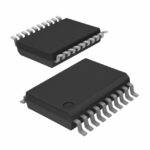 49FCT3805AQGI8
The activity of extra discounts on wholesale prices is in full swing…
Please fill in your contact information and we will send you the latest wholesale price list.






