 ChipApex | Global Electronic Components Supplier
SEARCH
Search Product
Search Post
— IC芯片 | 连接器 | 传感器 | 被动器件 —
Search productSearch post
— IC芯片 | 连接器 | 传感器 | 被动器件 —
Consult the customer manager about the wholesale price.
consultation hotline:86-132-6715-2157
email:[email protected]
Contact the product manager for consultation. One-stop consultation is available.
Do you want a lower wholesale price? Please send us your inquiry and we will reply immediately.
The Renesas Electronics Corporation 49FCT3805BPYG8 is a dual 1-to-5 clock driver and distribution buffer belonging to the 49FCT series. It operates on a single 3V to 3.6V power supply and utilizes advanced dual metal CMOS technology. The device features two independent driver banks, each providing a 1:5 fanout with individual output enable controls. It supports LVCMOS input and output logic levels and is housed in a 20-pin SSOP package. Designed for high-speed clock distribution, it ensures signal integrity and low skew.
Verify the specific suffix 'PYG8' against the manufacturer's current datasheet to confirm package dimensions and tape-and-reel specifications. Ensure compatibility with the required operating temperature range and voltage levels before integration into the design.
Select this component when a dual-bank clock distribution solution with independent enable controls is required. The inclusion of a dedicated monitor output makes it suitable for systems needing real-time diagnostic feedback on clock signal health. Verify that the 20-SSOP package fits the available PCB footprint constraints.
This part is part of the broader 49FCT3805 family, which includes variants such as the 49FCT3805APYGI8 and 49FCT3805ASOGI8. These components share the core 1:5 fanout functionality but differ in packaging options like SOIC or SSOP and environmental ratings. The BPYG8 variant specifically denotes the SSOP package configuration.
Direct replacements include other 49FCT3805 variants from Renesas with compatible pinouts and electrical characteristics. Cross-manufacturer alternatives may require verification of logic level compatibility and output drive strength.
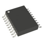 49FCT3805BPYG8
The activity of extra discounts on wholesale prices is in full swing…
Please fill in your contact information and we will send you the latest wholesale price list.






