 ChipApex | Global Electronic Components Supplier
SEARCH
Search Product
Search Post
— IC芯片 | 连接器 | 传感器 | 被动器件 —
Search productSearch post
— IC芯片 | 连接器 | 传感器 | 被动器件 —
Consult the customer manager about the wholesale price.
consultation hotline:86-132-6715-2157
email:[email protected]
Contact the product manager for consultation. One-stop consultation is available.
Do you want a lower wholesale price? Please send us your inquiry and we will reply immediately.
The 49FCT3805DPYGI8 is a dual 1-to-5 clock driver manufactured by Renesas Electronics. It operates on a single 3V to 3.6V supply and features LVCMOS input and output types. The device includes two independent driver banks, each with its own output enable control. It incorporates a heartbeat monitor for diagnostics and PLL driving, providing a MON output identical to other outputs. Designed for high-speed clock distribution, it ensures low skew and high signal quality. The component is housed in a 20-SSOP package and supports surface mount installation.
Verify the specific suffix 'D' against official Renesas documentation to confirm industrial temperature rating or specific manufacturing lot details, as standard variants may differ. Confirm RoHS compliance status directly from the manufacturer's datasheet before procurement. Ensure the SSOP-20 footprint matches the target PCB design constraints.
Select this component when dual independent clock buffers are required with diagnostic capabilities. The 1:5 fanout ratio suits distributing a single clock source to five loads. Verify that the 3V-3.6V operating voltage aligns with the system power rails. The LVCMOS interface compatibility should be confirmed against the connected logic family specifications.
This part belongs to the 49FCT series of Fast CMOS clock drivers. It is functionally related to the 49FCT3805A and 49FCT3805Q variants, differing primarily in package type (SSOP vs QSOP/SOIC) and potentially temperature grade indicated by the 'D' suffix. The series is designed for high-performance clock distribution in digital systems.
Publicly documented substitutes include Diodes Incorporated PI49FCT32805QE. Verify pinout compatibility and electrical parameters such as propagation delay and drive strength before substitution. Other 49FCT3805 variants with different packages may serve as physical replacements if electrical specs match.
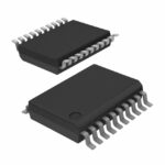 49FCT3805DPYGI8
The activity of extra discounts on wholesale prices is in full swing…
Please fill in your contact information and we will send you the latest wholesale price list.






