 ChipApex | Global Electronic Components Supplier
SEARCH
Search Product
Search Post
— IC芯片 | 连接器 | 传感器 | 被动器件 —
Search productSearch post
— IC芯片 | 连接器 | 传感器 | 被动器件 —
Consult the customer manager about the wholesale price.
consultation hotline:86-132-6715-2157
email:[email protected]
Contact the product manager for consultation. One-stop consultation is available.
Do you want a lower wholesale price? Please send us your inquiry and we will reply immediately.
The 49FCT3805QGI8 is a dual 1-to-5 clock driver manufactured by Renesas Electronics. It operates on a single 3V to 3.6V supply and utilizes advanced CMOS technology. The device integrates two independent driver banks, each providing five outputs with individual output enable controls. It features low capacitance inputs and includes a heartbeat monitor for diagnostics and PLL driving. The component is housed in a 20-pin QSOP package and supports LVCMOS/LVTTL input and output levels.
Verify the specific suffix GI8 corresponds to the 20-pin QSOP package and Reel/Cut Tape packaging options. Confirm RoHS compliance status through official datasheets or manufacturer notices before integration. Check for any Product Change Notices (PCN) regarding assembly source or material updates that may affect long-term availability.
Select this component when dual independent clock buffers are required in a compact QSOP footprint. Ensure the design environment supports the 3V to 3.6V operating voltage. Verify that the load capacitance requirements align with the FCT3805 drive capabilities. Consider the 49FCT3805D-E variant if a heartbeat monitor is not needed for the specific application.
This part belongs to the 49FCT3805Q family of clock drivers. It shares core functionality with variants such as the 49FCT3805APYGI8 (SSOP package) and 49FCT3805ASOGI8 (SOIC package). The primary distinction lies in the physical package type and associated pin-out dimensions, while maintaining identical electrical performance characteristics.
Publicly confirmed substitute part numbers are not available in the provided documentation. Cross-referencing requires verification of package compatibility and electrical parameter matching against alternative manufacturers' offerings.
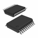 49FCT3805QGI8
The activity of extra discounts on wholesale prices is in full swing…
Please fill in your contact information and we will send you the latest wholesale price list.






