 ChipApex | Global Electronic Components Supplier
SEARCH
Search Product
Search Post
— IC芯片 | 连接器 | 传感器 | 被动器件 —
Search productSearch post
— IC芯片 | 连接器 | 传感器 | 被动器件 —
Consult the customer manager about the wholesale price.
consultation hotline:86-132-6715-2157
email:[email protected]
Contact the product manager for consultation. One-stop consultation is available.
Do you want a lower wholesale price? Please send us your inquiry and we will reply immediately.
The Renesas 49FCT805BTQG is a dual clock driver and distribution buffer belonging to the 49FCT series. It features a 1:5 multiplication factor with CMOS, LVCMOS, and TTL output types. The device supports a maximum output frequency of 166 MHz and accepts an LVCMOS input signal. Operating at a minimum supply voltage of 5 V, it functions within a commercial temperature range of 0°C to +70°C. The component is housed in a 20-pin SOIC package and draws a typical operating current of 33.5 mA.
Verify component authenticity through authorized distributors or direct manufacturer channels due to potential availability constraints. Confirm RoHS compliance status and specific packaging requirements prior to order placement. Ensure that the selected variant matches the required pinout and electrical specifications for the target application design.
Select this component when dual-channel clock buffering with mixed logic compatibility is required. Consider the 166 MHz speed limit and 5V operation for system integration. Evaluate thermal management needs based on the specified operating temperature range and power consumption characteristics during continuous duty cycles.
This part belongs to the Renesas 49FCT family of fast CMOS clock drivers. These components are engineered for high-performance clock distribution tasks in digital electronics. The 49FCT805 variant specifically addresses applications requiring simultaneous buffering of multiple clock domains with flexible output drive capabilities.
Public confirmed substitute part numbers include IDT49FCT805BTQ.
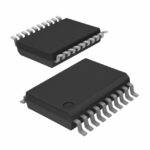 49FCT805BTQG
The activity of extra discounts on wholesale prices is in full swing…
Please fill in your contact information and we will send you the latest wholesale price list.





