 ChipApex | Global Electronic Components Supplier
SEARCH
Search Product
Search Post
— IC芯片 | 连接器 | 传感器 | 被动器件 —
Search productSearch post
— IC芯片 | 连接器 | 传感器 | 被动器件 —
Consult the customer manager about the wholesale price.
consultation hotline:86-132-6715-2157
email:[email protected]
Contact the product manager for consultation. One-stop consultation is available.
Do you want a lower wholesale price? Please send us your inquiry and we will reply immediately.
The Renesas Electronics Corporation 49FCT806SOG8 is a Fast CMOS inverting buffer and clock driver. It features two independent output banks, each providing a 1:5 fanout from a TTL-compatible input. The device includes a dedicated monitor (MON) output for diagnostics and PLL driving. Key electrical specifications include a maximum propagation delay of 5.3 ns, guaranteed low skew under 700 ps, and high drive capability with -24 mA source and +64 mA sink currents. It operates within a commercial temperature range of 0°C to +70°C.
Verify component status as this part may be obsolete or end-of-life. Confirm package type matches the SOIC-20 footprint. Check RoHS compliance requirements against specific manufacturing date codes, as non-green parts have historically faced discontinuation notices.
Select this component when dual independent clock buffering with a diagnostic monitor is required. Ensure the load capacitance does not exceed 50 pF to maintain specified timing parameters. Verify that the 0°C to +70°C commercial temperature range meets the application's environmental constraints.
This device belongs to the FCT series of Fast CMOS logic components. It was originally manufactured by Integrated Device Technology (IDT), which was acquired by Renesas Electronics Corporation. The 'SOG8' suffix indicates a Small Outline IC package with tape and reel packaging.
Consult official manufacturer documentation for current cross-reference data. Due to potential obsolescence, verify if newer generations of clock drivers are available from Renesas Electronics Corporation.
The MON pin serves as a 'Heartbeat' monitor output. It provides an identical signal to the other outputs, allowing it to be used for diagnostics and PLL driving.
The device has two independent output banks controlled by active-low inputs OEA and OEB. When these inputs are High, the respective outputs enter a high-impedance state.
The maximum output skew (tSK(O)) between outputs of all banks in the same package is guaranteed to be less than 700 ps.
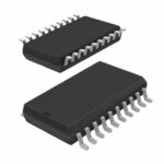 49FCT806SOG8
The activity of extra discounts on wholesale prices is in full swing…
Please fill in your contact information and we will send you the latest wholesale price list.





