 ChipApex | Global Electronic Components Supplier
SEARCH
Search Product
Search Post
— IC芯片 | 连接器 | 传感器 | 被动器件 —
Search productSearch post
— IC芯片 | 连接器 | 传感器 | 被动器件 —
Consult the customer manager about the wholesale price.
consultation hotline:86-132-6715-2157
email:[email protected]
Contact the product manager for consultation. One-stop consultation is available.
Do you want a lower wholesale price? Please send us your inquiry and we will reply immediately.
The Renesas 524SCMGI is a low skew, single input to four output LVCMOS clock buffer. It features an extremely low additive phase jitter of 50fs RMS and outputs with 50ps skew. The device supports input/output clock frequencies up to 200MHz and operates on supply voltages ranging from 1.8V to 3.3V. Packaged in an 8-UFDFN (2x2) surface mount format, it utilizes an advanced low-power CMOS process.
Verify the specific package variant against project requirements, as the 524S family includes SOIC and DFN options. Confirm that the 8-UFDFN footprint matches the PCB layout constraints. Ensure the operating voltage range aligns with the system power rails. Check the latest datasheet for any updates regarding moisture sensitivity levels or recommended soldering profiles.
Select this component when sub-50fs jitter performance is critical for signal integrity. The 8-UFDFN package offers a compact solution for space-constrained designs. Consider the 1.8V to 3.3V operating range compatibility with existing logic levels. Evaluate the 200MHz frequency limit against the target clock speed requirements.
The 524SCMGI belongs to the 524S series of low skew clock buffers manufactured by Renesas Electronics. This series is designed to provide precise clock distribution with minimal timing errors. The CMGI suffix specifically denotes the 8-UFDFN package type within the broader product line.
The 524SDCGI serves as a pin-compatible alternative within the same series, offering identical electrical specifications but packaged in an 8-SOIC format instead of the DFN configuration.
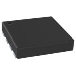 524SCMGI
The activity of extra discounts on wholesale prices is in full swing…
Please fill in your contact information and we will send you the latest wholesale price list.





