 ChipApex | Global Electronic Components Supplier
SEARCH
Search Product
Search Post
— IC芯片 | 连接器 | 传感器 | 被动器件 —
Search productSearch post
— IC芯片 | 连接器 | 传感器 | 被动器件 —
Consult the customer manager about the wholesale price.
consultation hotline:86-132-6715-2157
email:[email protected]
Contact the product manager for consultation. One-stop consultation is available.
Do you want a lower wholesale price? Please send us your inquiry and we will reply immediately.
The Renesas 551MLF is a low-cost, high-speed clock buffer featuring one input and four outputs. It belongs to the ClockBlocks family and utilizes an advanced CMOS process. The device operates within a supply voltage range of 3 V to 5.5 V and supports maximum input frequencies up to 160 MHz. Key electrical parameters include a maximum propagation delay of 8 ns. It is housed in an 8-pin SOIC package with surface-mount installation. The component functions as a non-inverting output clock buffer suitable for general timing applications.
Verify the specific suffix 'MLF' against official Renesas documentation to confirm package type and temperature grade. Ensure compatibility with the required operating voltage range of 3 V to 5.5 V. Confirm that the 8-lead SOIC package dimensions meet the target PCB layout constraints before finalizing procurement decisions.
Select this component when a low-cost, single-input to four-output clock buffer is required. It is appropriate for designs needing up to 160 MHz operation with a 3 V to 5.5 V supply. Consider the 8 ns propagation delay and SOIC-8 package form factor during schematic capture and layout planning.
The 551MLF is part of the Renesas 551 series, classified as a ClockBlocks family member. This series represents a line of low-cost, small-form-factor clock buffers designed for efficient signal distribution without complex phase-locked loop functionality.
Publicly confirmed substitute part numbers are not available in the provided source material.
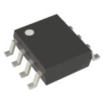 551MLF
The activity of extra discounts on wholesale prices is in full swing…
Please fill in your contact information and we will send you the latest wholesale price list.





