 ChipApex | Global Electronic Components Supplier
SEARCH
Search Product
Search Post
— IC芯片 | 连接器 | 传感器 | 被动器件 —
Search productSearch post
— IC芯片 | 连接器 | 传感器 | 被动器件 —
Consult the customer manager about the wholesale price.
consultation hotline:86-132-6715-2157
email:[email protected]
Contact the product manager for consultation. One-stop consultation is available.
Do you want a lower wholesale price? Please send us your inquiry and we will reply immediately.
The 553SCMGI8 is a low skew, single-input to four-output LVCMOS clock buffer from Renesas Electronics. It operates within a supply voltage range of 1.71 V to 3.465 V and supports maximum input frequencies up to 200 MHz. The device features sub-50 fs additive phase jitter performance. It utilizes an advanced, low-power CMOS process and is available in an 8-VFQFN (2x2) surface-mount package. The component is rated for extended industrial operating temperatures ranging from -40 °C to +105 °C.
Verify the specific suffix 'GI8' against the official datasheet to confirm packaging details, such as reel quantity and tape specifications. Confirm RoHS compliance status and moisture sensitivity level (MSL) ratings prior to integration into PCB assembly processes to ensure manufacturing reliability.
Select this component when sub-50 fs jitter performance is required for LVCMOS clock distribution. Ensure the design accommodates the 1.71 V to 3.465 V supply range. Verify that the 8-VFQFN package dimensions fit the board layout constraints compared to alternative packages like SOIC or DCGI.
This part belongs to the 553S series of clock buffers. It serves as a high-performance alternative to standard clock drivers by offering superior jitter characteristics. The device is designed to replace older generation buffers in applications demanding tight timing margins and low power consumption.
The 551SCMGI8 is listed as a parameter-equivalent substitute. Verify pinout compatibility and electrical specifications before substitution.
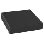 553SCMGI8
The activity of extra discounts on wholesale prices is in full swing…
Please fill in your contact information and we will send you the latest wholesale price list.





