 ChipApex | Global Electronic Components Supplier
SEARCH
Search Product
Search Post
— IC芯片 | 连接器 | 传感器 | 被动器件 —
Search productSearch post
— IC芯片 | 连接器 | 传感器 | 被动器件 —
Consult the customer manager about the wholesale price.
consultation hotline:86-132-6715-2157
email:[email protected]
Contact the product manager for consultation. One-stop consultation is available.
Do you want a lower wholesale price? Please send us your inquiry and we will reply immediately.
The Analog Devices DAC8412 is a quad, 12-bit voltage output digital-to-analog converter with readback capability. Built using a complementary BiCMOS process, it offers high package density in 28-lead PLCC, LCC, DIP, and CERDIP packages. The device supports operation from single +5 V to ±15 V supplies. Key electrical characteristics include a typical settling time of 10 μs to 0.01% for a 10 V step, integral nonlinearity error of ±1 LSB (F grade), and differential nonlinearity error of -1 LSB. Power dissipation is less than 330 mW with ±15 V supplies.
Verify the specific grade (E or F) and package type (PLCC, LCC, PDIP, or CERDIP) required for the MIL-STD-883 compliant part number 5962-9176404MXA against the manufacturer's ordering guide. Confirm temperature range specifications (-40°C to +85°C for commercial grades vs. -55°C to +125°C for military grades) match the application environment requirements.
Select this component when a quad-channel 12-bit DAC with parallel interface and readback functionality is needed. Ensure the system can accommodate the required reference voltages (VREFH/VREFL) and supply rails (+5 V to ±15 V). Consider the 10 μs settling time and ±1 LSB linearity for precision applications. Verify that the 28-lead PLCC or LCC footprint fits the PCB layout constraints.
The 5962-9176404MXA is a military-grade variant of the DAC8412 family, available on Standard Military Drawings. It shares the same functional architecture as the commercial DAC8412 but adheres to stricter reliability and environmental standards (MIL-STD-883). It is part of a series including the DAC8413, which differs only in its reset behavior (zero scale vs. midscale).
Public confirmed substitute part numbers are not provided in the source material.
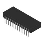 5962-9176404MXA
The activity of extra discounts on wholesale prices is in full swing…
Please fill in your contact information and we will send you the latest wholesale price list.





