 ChipApex | Global Electronic Components Supplier
SEARCH
Search Product
Search Post
— IC芯片 | 连接器 | 传感器 | 被动器件 —
Search productSearch post
— IC芯片 | 连接器 | 传感器 | 被动器件 —
Consult the customer manager about the wholesale price.
consultation hotline:86-132-6715-2157
email:[email protected]
Contact the product manager for consultation. One-stop consultation is available.
Do you want a lower wholesale price? Please send us your inquiry and we will reply immediately.
The Altera 5AGXBA7D4F31C5N is an Arria V GX Field Programmable Gate Array (FPGA) designed for high-performance digital logic applications. It features a capacity of 156,000 Logic Elements and 58,900 Adaptive Logic Modules within its architecture. The device integrates 10.26 Mbit of embedded memory and provides 416 I/O pins for system connectivity. Operating at a maximum frequency of 1.05 GHz, it supports data rates up to 6.5536 Gb/s via nine transceivers. The component functions at a supply voltage of 1.1 V and is housed in an 896-pin FBGA package suitable for surface mount technology.
Verify the specific suffix C5N against official datasheets to confirm temperature range and performance grade. Confirm RoHS compliance status through manufacturer documentation prior to integration. Check for obsolescence notices as this series may have limited availability. Ensure ESD protection protocols are followed during handling due to the fine-pitch FBGA packaging.
Compare the 156,000 LE count against design requirements to ensure sufficient logic resources. Evaluate the nine transceiver pairs against bandwidth needs for serial interface implementation. Verify that the 896-pin FBGA footprint matches the PCB layout constraints. Consider the 1.1 V power supply requirement for appropriate voltage regulation design.
This component belongs to the Arria V GX family, which targets cost-sensitive yet high-performance applications. The F31 designation indicates the specific 896-pin package variant used in this part number. The series is known for balancing logic density with efficient power consumption compared to larger FPGA families.
Direct substitutes within the same package and pinout include other Arria V GX variants such as 5AGXBA7D4F31C4G or 5AGXBA7D4F31I5, provided electrical specifications match. Cross-family migration to Cyclone V or Arria 10 requires schematic redesign and pin reassignment.


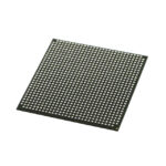 5AGXBA7D4F31C5N
The activity of extra discounts on wholesale prices is in full swing…
Please fill in your contact information and we will send you the latest wholesale price list.



