 ChipApex | Global Electronic Components Supplier
SEARCH
Search Product
Search Post
— IC芯片 | 连接器 | 传感器 | 被动器件 —
Search productSearch post
— IC芯片 | 连接器 | 传感器 | 被动器件 —
Consult the customer manager about the wholesale price.
consultation hotline:86-132-6715-2157
email:[email protected]
Contact the product manager for consultation. One-stop consultation is available.
Do you want a lower wholesale price? Please send us your inquiry and we will reply immediately.
The Altera 5AGXBB1D4F35C4N is an Arria V GX Field Programmable Gate Array (FPGA) designed for high-performance digital signal processing and communication applications. This device features a logic density of approximately 190,000 Logic Elements (LEs) and includes 544 I/O pins. It integrates embedded memory resources totaling 13,284,352 bits and supports up to 18 transceivers operating at speeds up to 12.5 Gbps. The component operates within a supply voltage range of 1.07V to 1.13V and functions reliably across a junction temperature range of 0°C to 85°C. It is housed in a 1152-ball FineLine BGA package with a 35mm x 35mm footprint.
Verify the specific ordering suffix against current Intel/Altera documentation to confirm package type and commercial temperature grade. Confirm end-of-life status or obsolescence notices prior to design finalization. Ensure compatibility with existing PCB footprints and thermal management solutions during procurement planning.
Compare the 190k LE count and transceiver availability against project complexity requirements. Evaluate power consumption profiles relative to available cooling infrastructure. Consider alternative Arria V variants if higher logic density or different pin counts are required for system integration.
This component belongs to the Arria V GX family, which targets cost-sensitive high-performance applications. It shares architectural similarities with other Arria V devices but offers specific I/O and transceiver configurations tailored for general-purpose high-speed connectivity and signal processing tasks within the Altera portfolio.
Direct substitutes may include other Arria V GX parts with similar logic densities such as 5AGXBB3 series variants. Verify pin-to-pin compatibility and electrical specifications before considering migration to newer Agilex families.


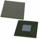 5AGXBB1D4F35C4N
The activity of extra discounts on wholesale prices is in full swing…
Please fill in your contact information and we will send you the latest wholesale price list.




