 ChipApex | Global Electronic Components Supplier
SEARCH
Search Product
Search Post
— IC芯片 | 连接器 | 传感器 | 被动器件 —
Search productSearch post
— IC芯片 | 连接器 | 传感器 | 被动器件 —
Consult the customer manager about the wholesale price.
consultation hotline:86-132-6715-2157
email:[email protected]
Contact the product manager for consultation. One-stop consultation is available.
Do you want a lower wholesale price? Please send us your inquiry and we will reply immediately.
The Altera 5AGXBB1D6F31C6G is an Arria V GX Field Programmable Gate Array (FPGA) integrated circuit. It features 362,000 logic elements and 17,110 Adaptive Logic Modules (ALMs). The device includes 19,822,592 total RAM bits for embedded memory applications. It provides 384 input/output pins and operates within a supply voltage range of 1.07V to 1.13V. The component is housed in an 896-ball Fine-Pitch Ball Grid Array (FCBGA) package with dimensions of 31x31 mm. It supports a maximum data rate of 6.5536 Gb/s via its transceivers and functions at junction temperatures between 0°C and 85°C.
Verify the specific ordering suffix against official manufacturer documentation to confirm temperature grade and package variant. Ensure compatibility with existing board layouts by cross-referencing pin assignments and mechanical dimensions. Confirm RoHS compliance status through current datasheets before finalizing procurement specifications.
Select this model when system requirements align with the 362,000 logic element capacity and 384 I/O count. Evaluate power consumption profiles against the specified 1.07V to 1.13V operating range. Consider the 896-ball FCBGA footprint constraints during PCB design phase to ensure adequate routing space and thermal management solutions.
This component belongs to the Altera Arria V GX family, which targets cost-sensitive yet performance-demanding applications. The series combines significant logic density with embedded memory blocks and high-speed transceivers. It serves as a scalable solution for designs requiring moderate to high throughput without the complexity of larger Stratix devices.
Direct substitutes include other variants within the Arria V GX family sharing the same 896-ball FCBGA package and pinout, such as 5AGXBB3D6F31C6G or 5AGXBB5D6F31C6G. Verify functional equivalence regarding logic resources and memory size before substitution.
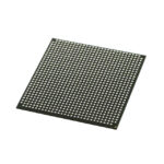 5AGXBB1D6F31C6G
The activity of extra discounts on wholesale prices is in full swing…
Please fill in your contact information and we will send you the latest wholesale price list.






