 ChipApex | Global Electronic Components Supplier
SEARCH
Search Product
Search Post
— IC芯片 | 连接器 | 传感器 | 被动器件 —
Search productSearch post
— IC芯片 | 连接器 | 传感器 | 被动器件 —
Consult the customer manager about the wholesale price.
consultation hotline:86-132-6715-2157
email:[email protected]
Contact the product manager for consultation. One-stop consultation is available.
Do you want a lower wholesale price? Please send us your inquiry and we will reply immediately.
The Altera 5AGXBB7D4F35I5N is an Arria V GX Field Programmable Gate Array (FPGA) manufactured using a 28nm low-power process. It features 300,000 logic elements and 113,208 Adaptive Logic Modules (ALMs). The device includes 14.75 Mbit of embedded memory and provides 544 I/Os. It integrates 24 transceivers with a maximum data rate of 6.5536 Gb/s. Operating at a core voltage of 1.1 V, it supports a maximum frequency of 1.05 GHz. The component is housed in an FBGA-1152 package and operates within a temperature range of -40°C to +100°C.
Verify the specific manufacturing date code and lot number upon receipt to ensure component authenticity. Confirm that the device has been stored under appropriate humidity-controlled conditions to prevent moisture damage prior to reflow soldering. Check for any physical defects on the FBGA-1152 package pins or substrate.
Compare the 300,000 LE capacity against design complexity to avoid resource over-provisioning. Ensure the 24 transceiver count meets all serial link requirements. Verify that the 1.1 V supply rail aligns with the system's power architecture and thermal management capabilities for the industrial temperature range.
This part belongs to the Arria V GX family, designed for cost-sensitive applications requiring moderate performance. It shares the FBGA-1152 footprint with other variants in the series, such as the 5AGXFA and 5AGXMA models, allowing for potential pin-compatible upgrades or downgrades depending on logic density needs.
Direct pin-compatible replacements within the same package include other Arria V GX devices like the 5AGXFB1H4F35I5N. However, logic element counts and memory configurations differ significantly between these variants. Validate timing closure and resource utilization before substituting.


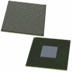 5AGXBB7D4F35I5N
The activity of extra discounts on wholesale prices is in full swing…
Please fill in your contact information and we will send you the latest wholesale price list.



