 ChipApex | Global Electronic Components Supplier
SEARCH
Search Product
Search Post
— IC芯片 | 连接器 | 传感器 | 被动器件 —
Search productSearch post
— IC芯片 | 连接器 | 传感器 | 被动器件 —
Consult the customer manager about the wholesale price.
consultation hotline:86-132-6715-2157
email:[email protected]
Contact the product manager for consultation. One-stop consultation is available.
Do you want a lower wholesale price? Please send us your inquiry and we will reply immediately.
The Altera 5AGXMB1G4F35C4N is a Stratix V GX Field Programmable Gate Array (FPGA) featuring 1900 LABs and 432 I/Os. It utilizes a 65 nm process technology and operates within a supply voltage range of 1.07V to 1.13V. The device supports a maximum operating frequency of 1.05 GHz and includes embedded memory totaling 23,625,728 bits. It is housed in a 1152-ball FCBGA package with dimensions of 35x35 mm. The component is rated for commercial temperature ranges from 0°C to 85°C junction temperature.
Verify the exact ordering suffix against official Intel/Altera documentation to ensure correct package and temperature grade. Confirm end-of-life status with authorized distributors as availability may be limited. Request original manufacturer datasheets to validate electrical specifications before integration into production designs.
Compare total LAB count and transceiver capabilities against current design requirements. Ensure the 1152-FBGA package fits within the target PCB footprint constraints. Verify that the 1.1V core voltage aligns with existing power delivery network designs on the target hardware platform.
This component belongs to the Stratix V family, representing a high-density FPGA solution from Altera. It serves as a successor to earlier generations, offering improved performance per watt. The specific model targets applications needing substantial logic resources combined with high-speed serial connectivity capabilities.
Check for direct pin-compatible upgrades within the Stratix V lineup. Consider Agilex series devices for modernized feature sets if form factor allows redesign. Consult official migration guides for architectural differences when transitioning to newer FPGA families.


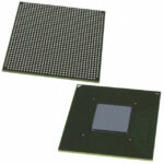 5AGXMB1G4F35C4N
The activity of extra discounts on wholesale prices is in full swing…
Please fill in your contact information and we will send you the latest wholesale price list.



