 ChipApex | Global Electronic Components Supplier
SEARCH
Search Product
Search Post
— IC芯片 | 连接器 | 传感器 | 被动器件 —
Search productSearch post
— IC芯片 | 连接器 | 传感器 | 被动器件 —
Consult the customer manager about the wholesale price.
consultation hotline:86-132-6715-2157
email:[email protected]
Contact the product manager for consultation. One-stop consultation is available.
Do you want a lower wholesale price? Please send us your inquiry and we will reply immediately.
The Altera 5AGXMB1G4F40I5N is an Arria V GX Field Programmable Gate Array (FPGA) manufactured using a 28nm low-power process. It features 300,000 logic elements and 11,320 Adaptive Logic Modules (ALMs). The device integrates 14.75 Mbit of embedded memory, comprising distributed RAM and embedded block RAM. It provides 384 I/Os and includes 18 high-speed transceivers capable of data rates up to 6.5536 Gb/s. Operating at a maximum frequency of 1.05 GHz, it supports supply voltages between 1.15V and 1.15V for the core. The component is housed in an 896-pin FBGA package with dimensions of 30x30mm and operates within a junction temperature range of -40°C to +100°C.
Verify the specific manufacturing date code and lot number against the datasheet revision history to ensure compliance with current RoHS and REACH regulations. Confirm that the device has not been exposed to moisture beyond its specified humidity sensitivity level prior to soldering. Request a certificate of conformity from the supplier to validate authenticity and traceability through the authorized distribution channel.
Select this model when the design requires a balance of moderate logic density and significant serial connectivity. The presence of 18 transceivers makes it suitable for applications needing multiple high-speed interfaces. Ensure the PCB layout accommodates the 896-ball BGA footprint and thermal requirements associated with the 28nm process node under industrial temperature conditions.
This component belongs to the Arria V GX family, which targets cost-sensitive applications requiring high performance. It serves as a bridge between lower-density CPLDs and larger Stratix FPGAs. The 'GX' designation indicates the inclusion of high-speed transceivers, distinguishing it from the standard Arria V series. It is designed for environments where power efficiency and moderate I/O counts are critical constraints.
Direct pin-to-pin replacements are limited within the Altera portfolio due to varying pin counts and feature sets. Consider the 5AGXMB1G4F31I3N for similar functionality but with different speed grades or package options. Verify compatibility with existing Quartus Prime software versions, as newer tool releases may drop support for older device families.


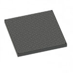 5AGXMB1G4F40I5N
The activity of extra discounts on wholesale prices is in full swing…
Please fill in your contact information and we will send you the latest wholesale price list.



