 ChipApex | Global Electronic Components Supplier
SEARCH
Search Product
Search Post
— IC芯片 | 连接器 | 传感器 | 被动器件 —
Search productSearch post
— IC芯片 | 连接器 | 传感器 | 被动器件 —
Consult the customer manager about the wholesale price.
consultation hotline:86-132-6715-2157
email:[email protected]
Contact the product manager for consultation. One-stop consultation is available.
Do you want a lower wholesale price? Please send us your inquiry and we will reply immediately.
The 5P83904CMGK is a high-performance clock buffer manufactured by Renesas Electronics. It functions as a 1-to-4 fanout buffer with a crystal input and LVCMOS outputs. The device accepts fundamental mode crystals in the 10 MHz to 40 MHz range and provides four LVCMOS clock outputs. Key electrical specifications include a maximum propagation delay of 6 ns, an operating supply voltage range of 1.71 V to 3.465 V, and a typical operating current of 12.1 mA. It is housed in a QFN-16 package and supports an industrial temperature range from -40°C to +105°C.
Verify the specific suffix 'CMGK' against the official datasheet to confirm the package type (QFN-16) and temperature grade. Ensure compatibility with the required crystal frequency range of 10 MHz to 40 MHz. Check for RoHS compliance status as indicated in the manufacturer's documentation before finalizing procurement.
Select this component when a single crystal input needs to drive four LVCMOS loads with minimal skew. The glitch-free output enable feature is critical for applications requiring clean clock transitions during power-up or shutdown. Verify that the system supply voltage falls within the 1.71 V to 3.465 V range and that the thermal requirements fit the -40°C to +105°C operational window.
This part belongs to the 5P8390x family of mixed-signal clock buffers. The 'C' in the part number typically denotes the industrial temperature range (-40°C to +105°C), while 'MGK' specifies the QFN-16 package variant. It serves as a specialized timing solution distinct from general-purpose logic buffers due to its integrated crystal input handling capabilities.
Consult the official Renesas selection guide for direct pin-compatible alternatives within the 5P8390x series. Verify if other suffixes such as 'PGGK' (TSSOP-16) meet mechanical constraints. No third-party substitutes are confirmed in public documentation; cross-referencing with the manufacturer's obsolescence notices is recommended.
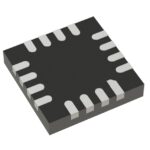 5P83904CMGK
The activity of extra discounts on wholesale prices is in full swing…
Please fill in your contact information and we will send you the latest wholesale price list.






