 ChipApex | Global Electronic Components Supplier
SEARCH
Search Product
Search Post
— IC芯片 | 连接器 | 传感器 | 被动器件 —
Search productSearch post
— IC芯片 | 连接器 | 传感器 | 被动器件 —
Consult the customer manager about the wholesale price.
consultation hotline:86-132-6715-2157
email:[email protected]
Contact the product manager for consultation. One-stop consultation is available.
Do you want a lower wholesale price? Please send us your inquiry and we will reply immediately.
The 5P83908NDGK is a high-performance clock fanout buffer manufactured by Renesas Electronics. It accepts a crystal input and provides eight LVCMOS outputs with a 1:8 distribution ratio. The device supports maximum frequencies of 200 MHz and operates on a supply voltage ranging from 1.71 V to 3.465 V. It features a maximum propagation delay of 6 ns and functions within an operating temperature range of -40°C to +105°C. The component is housed in a surface-mount 20-VFQFN package with an exposed pad, measuring 3x3 mm.
Verify the specific suffix NDGK to confirm the 20-VFQFN package configuration, as other suffixes indicate different physical footprints. Ensure the application environment remains within the specified -40°C to +105°C operational temperature limits. Confirm that the power supply voltage stays strictly between 1.71 V and 3.465 V to prevent device malfunction or damage during operation.
Select this component when a single crystal source must drive multiple downstream loads simultaneously. The 1:8 ratio makes it suitable for distributing a master clock to several synchronous devices. Consider the 200 MHz frequency limit and LVCMOS output compatibility when matching requirements against connected circuitry specifications.
This part belongs to the 5P83908 series of mixed-signal clock buffers designed for high-performance applications. It serves as a critical timing element in complex electronic architectures where precise clock distribution is required. The series offers various package options to accommodate different board space and thermal management constraints.
The 5P83908PGGK is a confirmed substitute offering identical electrical performance but utilizing a 20-TSSOP package instead of the QFN form factor.
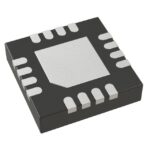 5P83908NDGK
The activity of extra discounts on wholesale prices is in full swing…
Please fill in your contact information and we will send you the latest wholesale price list.






