 ChipApex | Global Electronic Components Supplier
SEARCH
Search Product
Search Post
— IC芯片 | 连接器 | 传感器 | 被动器件 —
Search productSearch post
— IC芯片 | 连接器 | 传感器 | 被动器件 —
Consult the customer manager about the wholesale price.
consultation hotline:86-132-6715-2157
email:[email protected]
Contact the product manager for consultation. One-stop consultation is available.
Do you want a lower wholesale price? Please send us your inquiry and we will reply immediately.
The Renesas Electronics 5PB1102CMGK is a high-performance 1:2 LVCMOS clock buffer designed for low-jitter clock distribution. It operates from a single supply voltage ranging from 1.8V to 3.3V and supports maximum frequencies up to 200MHz. The device features an integrated serial termination for 50Ω channels, ensuring signal integrity in high-speed applications. Key performance metrics include very low pin-to-pin skew of less than 50ps and additive jitter below 50fs RMS. It includes an Output Enable function and is available in an 8-lead DFN package with dimensions of 2.0mm x 2.0mm.
Verify the specific suffix 'K' against official documentation to confirm the extended temperature range (-40°C to +105°C) compared to standard variants. Confirm package type as 8-DFN (2x2 mm). Check current availability status as stock levels may vary by region and distributor.
Select this component when ultra-low jitter is critical for system performance. Ensure the design requires a 1:2 fanout ratio with LVCMOS outputs. Verify that the PCB layout can accommodate the small 2x2mm DFN footprint and that the operating environment falls within the specified temperature range for the 'K' suffix variant.
The 5PB1102CMGK belongs to the 5PB11xx series of ultra-low jitter LVCMOS buffers manufactured by Renesas Electronics. This series is engineered to replace traditional clock drivers in noise-sensitive digital systems, offering superior phase noise performance compared to standard logic buffers while maintaining low power consumption.
Direct substitutes include other 1:2 LVCMOS clock buffers with similar jitter specifications (<50fs) and supply voltage ranges (1.8V-3.3V). Verify pin compatibility and thermal characteristics before substitution.
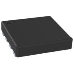 5PB1102CMGK
The activity of extra discounts on wholesale prices is in full swing…
Please fill in your contact information and we will send you the latest wholesale price list.




