 ChipApex | Global Electronic Components Supplier
SEARCH
Search Product
Search Post
— IC芯片 | 连接器 | 传感器 | 被动器件 —
Search productSearch post
— IC芯片 | 连接器 | 传感器 | 被动器件 —
Consult the customer manager about the wholesale price.
consultation hotline:86-132-6715-2157
email:[email protected]
Contact the product manager for consultation. One-stop consultation is available.
Do you want a lower wholesale price? Please send us your inquiry and we will reply immediately.
The 5PB1104CMGK is a high-performance LVCMOS clock buffer manufactured by Renesas Electronics Corporation. It features a 1:4 input-to-output ratio with a maximum operating frequency of 200 MHz. The device operates within supply voltage ranges of 1.71V to 1.89V, 2.375V to 2.625V, and 3.135V to 3.465V. Packaged in an 8-VFQFN (2x2 mm) surface-mount format, it supports an extended industrial temperature range from -40°C to +105°C. The component utilizes LVCMOS input and output logic levels.
Verify the specific suffix 'K' corresponds to the required tape-and-reel packaging configuration. Confirm that the 8-VFQFN footprint matches the PCB layout constraints. Ensure the selected supply voltage aligns with one of the three supported operational ranges. Check for RoHS3 compliance status if environmental regulations apply to the final assembly.
Select this component when a single-ended LVCMOS source requires fan-out to four loads without differential signaling. Compare against the 5PB1104PGGK if a TSSOP-8 package is preferred over the QFN form factor. Consider the 5PB1102 series if only two outputs are sufficient for the design requirements.
This part belongs to the 5PB11xx family of ultra-low jitter LVCMOS buffers. These components are designed to replace legacy discrete transistor solutions or older buffer ICs in modern mixed-signal environments. The 5PB1104 variant specifically addresses the need for quad fan-out in compact footprints.
Publicly documented parameter-equivalent substitutes include the 5PB1104CMGK/W and the 651SCMGI8. Verify pin compatibility and electrical specifications before substituting.
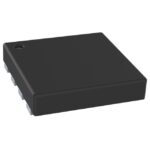 5PB1104CMGK
The activity of extra discounts on wholesale prices is in full swing…
Please fill in your contact information and we will send you the latest wholesale price list.





