 ChipApex | Global Electronic Components Supplier
SEARCH
Search Product
Search Post
— IC芯片 | 连接器 | 传感器 | 被动器件 —
Search productSearch post
— IC芯片 | 连接器 | 传感器 | 被动器件 —
Consult the customer manager about the wholesale price.
consultation hotline:86-132-6715-2157
email:[email protected]
Contact the product manager for consultation. One-stop consultation is available.
Do you want a lower wholesale price? Please send us your inquiry and we will reply immediately.
The Renesas Electronics 5PB1104PGGK is a high-performance clock buffer featuring four LVCMOS outputs. It operates within a supply voltage range of 1.71 V to 3.465 V and supports maximum input frequencies up to 200 MHz. The device exhibits a maximum propagation delay of 2.4 ns and draws 20 mA during operation. Packaged in an 8-pin TSSOP, it functions reliably across an extended temperature range from -40 °C to +105 °C.
Verify the specific suffix PGGK against official datasheets to confirm the TSSOP-8 package and lead-free status. Confirm RoHS compliance details directly with the manufacturer documentation as standard packaging may vary by region.
Select this component when a single-input, four-output LVCMOS buffer is required. Ensure the design accommodates the 1.71 V to 3.465 V supply range and that the 2.4 ns propagation delay meets system timing constraints.
This part belongs to the 5PB11xx series of ultra-low jitter LVCMOS buffers originally developed by IDT and integrated into Renesas Electronics' portfolio. The series provides high-performance clock buffering solutions for demanding digital applications.
The 5PB1104CMT1 serves as a compatible alternative within the same family, offering identical electrical specifications but utilizing a Cut Tape packaging format instead of the Tube configuration found in the PGGK variant.
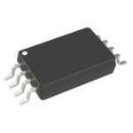 5PB1104PGGK
The activity of extra discounts on wholesale prices is in full swing…
Please fill in your contact information and we will send you the latest wholesale price list.





