 ChipApex | Global Electronic Components Supplier
SEARCH
Search Product
Search Post
— IC芯片 | 连接器 | 传感器 | 被动器件 —
Search productSearch post
— IC芯片 | 连接器 | 传感器 | 被动器件 —
Consult the customer manager about the wholesale price.
consultation hotline:86-132-6715-2157
email:[email protected]
Contact the product manager for consultation. One-stop consultation is available.
Do you want a lower wholesale price? Please send us your inquiry and we will reply immediately.
The 5PB1106CMGK is a clock fanout buffer manufactured by Renesas Electronics. It accepts one LVCMOS input and distributes the signal to six LVCMOS outputs, providing a 1:6 ratio. The device supports maximum frequencies of 200 MHz with a typical propagation delay of 2.7 ns. It operates within supply voltage ranges of 1.71V to 1.89V, 2.375V to 2.625V, or 3.135V to 3.465V. The component is housed in a 16-UFQFN package (2.5x2.5 mm) and functions across an industrial temperature range of -40°C to 105°C.
Verify the specific suffix CMGK corresponds to the 16-UFQFN package variant when sourcing. Confirm that the required operating voltage aligns with the supported 1.8V, 2.5V, or 3.3V rails. Ensure the thermal environment remains within the specified -40°C to 105°C range for reliable performance. Cross-reference the manufacturer datasheet for pin configuration details before integration.
Select this component when a single clock source must drive multiple loads without degradation. The 1:6 ratio suits applications requiring moderate fan-out capabilities. Consider the 16-UFQFN footprint for space-constrained designs. Verify compatibility with the system's logic voltage levels, as the device supports multiple LVCMOS standards.
This part belongs to the 5PB1106 series of mixed-signal clock buffers from Renesas. The series provides high-performance LVCMOS clock distribution solutions. The CMGK suffix specifically denotes the surface-mount QFN packaging option, distinguishing it from other package variants like TSSOP available in the same product family.
Direct substitutes include other 1:6 LVCMOS clock buffers from Renesas such as the 5PB1106PGGI, though package differences exist. Verify electrical parameters and pinout compatibility before swapping components.
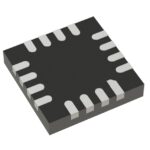 5PB1106CMGK
The activity of extra discounts on wholesale prices is in full swing…
Please fill in your contact information and we will send you the latest wholesale price list.





