 ChipApex | Global Electronic Components Supplier
SEARCH
Search Product
Search Post
— IC芯片 | 连接器 | 传感器 | 被动器件 —
Search productSearch post
— IC芯片 | 连接器 | 传感器 | 被动器件 —
Consult the customer manager about the wholesale price.
consultation hotline:86-132-6715-2157
email:[email protected]
Contact the product manager for consultation. One-stop consultation is available.
Do you want a lower wholesale price? Please send us your inquiry and we will reply immediately.
The 5PB1106CMGK8 is a high-performance clock buffer manufactured by Renesas Electronics, designed for precise signal distribution in mixed-signal environments. It features a 1:6 LVCMOS output configuration with a maximum operating frequency of 200 MHz. The device operates within a supply voltage range of 1.71 V to 3.465 V and exhibits a maximum propagation delay of 2.7 ns. Packaged in an 8-pin DFN format, it supports surface-mount installation and functions reliably across an extended temperature range from -40°C to +105°C.
Verify the specific suffix 'K8' against official Renesas documentation to confirm the package type and temperature grade, as suffixes often denote manufacturing lot or packaging variations. Confirm RoHS compliance status through the manufacturer's current datasheet, as regulatory statuses can change over time without immediate public notice.
Select this component when a single clock source must drive up to six LVCMOS loads with minimal skew. Ensure the system power supply remains stable between 1.71 V and 3.465 V. Verify that the required operating temperature does not exceed +105°C, as this part is rated for extended industrial conditions compared to commercial-grade alternatives.
This component belongs to the 5PB1106 series of clock buffers, which are optimized for low jitter and high performance. The series typically includes variants with different output counts and package styles, such as TSSOP or QFN options, allowing designers to choose form factors suitable for dense PCB layouts while maintaining signal integrity.
Direct replacements include other 5PB1106 variants like 5PB1106PGGI or 5PB1106NDGK, provided the package footprint and pinout compatibility are verified. Cross-model substitution requires careful evaluation of propagation delay and supply voltage specifications to ensure circuit functionality remains unaffected.
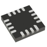 5PB1106CMGK8
The activity of extra discounts on wholesale prices is in full swing…
Please fill in your contact information and we will send you the latest wholesale price list.






