 ChipApex | Global Electronic Components Supplier
SEARCH
Search Product
Search Post
— IC芯片 | 连接器 | 传感器 | 被动器件 —
Search productSearch post
— IC芯片 | 连接器 | 传感器 | 被动器件 —
Consult the customer manager about the wholesale price.
consultation hotline:86-132-6715-2157
email:[email protected]
Contact the product manager for consultation. One-stop consultation is available.
Do you want a lower wholesale price? Please send us your inquiry and we will reply immediately.
The 5PB1110NDGI is a single-channel LVCMOS fanout buffer manufactured by Renesas Electronics. It provides a 1:10 input-to-output ratio, distributing a single clock signal to ten independent outputs. The device supports maximum frequencies of 200 MHz with a typical propagation delay of 2.5 ns. It operates within a supply voltage range of 1.71 V to 3.465 V and functions across an industrial temperature range of -40°C to +85°C. Packaged in a 20-VFQFN (3x3 mm) format with exposed pads, it draws approximately 40 mA of operating current.
Verify the specific suffix 'NDGI' against the manufacturer's datasheet to confirm the 20-VFQFN package type and the -40°C to +85°C temperature rating. Ensure that the ordering quantity aligns with the tray packaging specifications provided by authorized distributors. Cross-reference the RoHS compliance status and moisture sensitivity level prior to procurement to ensure compatibility with assembly processes.
Select the 5PB1110NDGI when a single-ended LVCMOS clock source requires expansion into ten identical output paths. This component is appropriate for designs operating between 1.71 V and 3.465 V where a 200 MHz maximum frequency is sufficient. Consider the 20-VFQFN footprint for PCB layout constraints. If differential inputs or higher drive currents are required, alternative buffer families should be evaluated.
This component belongs to the 5PB1110 series of clock buffers. The NDGI suffix specifically denotes the 20-VFQFN package variant with an extended industrial temperature range. Other variants in the series, such as those ending in PGGI, utilize TSSOP packages. The series is designed for general-purpose clock distribution in digital systems requiring LVCMOS compatibility.
The 5PB1110PGGK is identified as a parameter-equivalent replacement option available from Renesas. Verify pinout compatibility and package dimensions before substitution. Ensure that any alternative component meets the same 200 MHz frequency and voltage requirements.
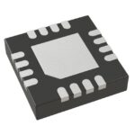 5PB1110NDGI
The activity of extra discounts on wholesale prices is in full swing…
Please fill in your contact information and we will send you the latest wholesale price list.




