 ChipApex | Global Electronic Components Supplier
SEARCH
Search Product
Search Post
— IC芯片 | 连接器 | 传感器 | 被动器件 —
Search productSearch post
— IC芯片 | 连接器 | 传感器 | 被动器件 —
Consult the customer manager about the wholesale price.
consultation hotline:86-132-6715-2157
email:[email protected]
Contact the product manager for consultation. One-stop consultation is available.
Do you want a lower wholesale price? Please send us your inquiry and we will reply immediately.
The 5PB1110NDGK8 is a high-performance clock buffer manufactured by Renesas Electronics. It functions as a 1:10 fanout buffer with LVCMOS input and output signaling. The device supports maximum frequencies of 200 MHz and operates within a supply voltage range of 1.71V to 3.465V, including specific nominal ranges for 1.8V, 2.5V, and 3.3V systems. It is housed in a 20-VFQFN package with exposed pad (3x3 mm) and is rated for an operating temperature range of -40°C to 105°C.
Verify the complete part number including the '8' suffix when ordering, as it indicates specific tape-and-reel packaging configurations distinct from tube or cut-tape variants. Confirm that the 20-VFQFN footprint matches the target PCB layout. Ensure the design accommodates the exposed thermal pad requirements for proper heat dissipation and electrical connection.
Select this component when a single LVCMOS clock source needs to drive ten downstream LVCMOS loads. The 1:10 ratio distinguishes it from other family members like the 5PB1102 (1:2). Verify that the required operating voltage falls within the specified 1.71V to 3.465V window. Consider the 20-VFQFN package constraints if space is limited compared to TSSOP options.
This part belongs to the Renesas 5PB11xx series of mixed-signal clock buffers. It shares the core 5PB1110 architecture but differs in packaging and shipping format. Other variants include the NDGI (tube), PGGI (TSSOP tube), and PGGI8 (TSSOP reel). The NDGK8 variant specifically utilizes the QFN form factor with reel packaging.
Direct pin-compatible replacements within the same manufacturer include the 5PB1110NDGI (same function/package, different packaging) and the 5PB1110PGGK (same function, TSSOP-20 package). Cross-manufacturer substitution requires verifying LVCMOS compatibility and 200 MHz performance limits.
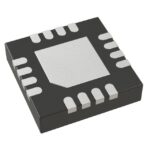 5PB1110NDGK8
The activity of extra discounts on wholesale prices is in full swing…
Please fill in your contact information and we will send you the latest wholesale price list.





