 ChipApex | Global Electronic Components Supplier
SEARCH
Search Product
Search Post
— IC芯片 | 连接器 | 传感器 | 被动器件 —
Search productSearch post
— IC芯片 | 连接器 | 传感器 | 被动器件 —
Consult the customer manager about the wholesale price.
consultation hotline:86-132-6715-2157
email:[email protected]
Contact the product manager for consultation. One-stop consultation is available.
Do you want a lower wholesale price? Please send us your inquiry and we will reply immediately.
The Renesas Electronics 5PB1110PGGK8 is a high-performance clock buffer and fan-out device belonging to the 5PB1110 series. It features one LVCMOS input and ten LVCMOS outputs, supporting maximum frequencies of 200 MHz for both input and output signals. The component operates within a supply voltage range of 1.71 V to 3.465 V and exhibits a maximum propagation delay of 2.5 ns. Packaged in a 20-TSSOP format with dimensions of 0.173 inches (4.40 mm) width, it is designed for surface mount installation. The device functions reliably across an extended industrial temperature range from -40°C to +85°C.
Verify the specific suffix 'K8' against official Renesas documentation to confirm packaging details, as this typically indicates tape-and-reel configuration. Ensure compatibility with existing PCB footprints for the 20-TSSOP package. Cross-reference RoHS compliance status directly with the manufacturer's current datasheet to meet regulatory requirements.
Select the 5PB1110PGGK8 when a design requires driving ten loads from a single clock source without differential signaling. This part is suitable for applications needing low skew and jitter performance within the LVCMOS domain. Compare against other members of the 5PB11xx family if different output counts or package sizes are required.
This component is part of the Renesas 5PB1110 series of clock buffers. The base model 5PB1110 defines the core electrical specifications, while the suffixes indicate variations in packaging and handling. The PGGI variant represents tube packaging, whereas the PGGK8 variant denotes reel packaging for automated assembly processes.
The 5PB1110PGGK is identified as a parameter-equivalent alternative available from Renesas Electronics. Verify pinout and electrical characteristics match before substitution.
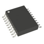 5PB1110PGGK8
The activity of extra discounts on wholesale prices is in full swing…
Please fill in your contact information and we will send you the latest wholesale price list.






